Introduction
In the SATA protocol, the essence of data transmission is the interaction of FIS (Frame Information Structure). Different FIS types are responsible for different aspects: some are for “notification”, some for “context configuration”, and others for “actual data transfer”. If we consider SATA as a highway, then these FIS are like traffic lights, road signs, and trucks along the way, ensuring that data can travel safely, orderly, and reliably between the Host and Device. This article will combine DMA Activate / DMA Setup / PIO Setup / Data FIS to clarify their roles, timing relationships, and design concepts, helping you to understand the data flow mechanism of SATA in both PIO and DMA modes.
DMA-Activate

A small signal specifically used in SATA to coordinate the DMA write (Host→Device) data flow.
What is its purpose?
- • When the Host wants to write data to the Device (DMA Write Command, such as
<span>WRITE DMA EXT</span>or<span>WRITE FPDMA QUEUED</span>), the data is sent via Data FIS (Host → Device). - • However, the Host cannot send Data FIS arbitrarily, it must wait for the Device to be ready and explicitly tell the Host, “You can send now”.
- • This “you can send now” signal is the DMA Activate FIS.
DMA Activate FIS = The “gate opening signal” sent from the Device to the Host, telling it that it can start sending the next batch of data.
Why is it needed?
- • Data may be sent in multiple batches: Some write requests are large, and one Data FIS cannot accommodate them, so they must be split into multiple Data FIS.
- • If the Host ignores the Device’s status and sends continuously, it may cause the Device to be unable to process in time, resulting in data loss.
- • Therefore, the SATA protocol requires that for each Data FIS sent by the Host, it must wait for a DMA Activate FIS from the Device before sending the next one.
- • This implements flow control, ensuring that both sides are synchronized.
Field meanings
- • PM Port: If using a Port Multiplier, it indicates which port the FIS comes from; for a directly connected hard drive, it is fixed at 0.
- • Reserved (R): Reserved field, must be set to 0.
- • No additional data, as it is just a “notification”.
Timing relationships
A typical DMA write process (Host → Device):
- 1. The Host sends a DMA Setup FIS (telling the Device how much data will be written and from where).
- 2. The Device replies with a DMA Activate FIS (I am ready, you can send data).
- 3. The Host sends a Data FIS (with data).
- 4. If there is more data to send, return to step 2 (wait for a new DMA Activate).
- 5. After all data is sent, the Device reports status/completion using Register D2H FIS or Set Device Bits FIS.
Protocol design points
- • Ensure reliability: The Host will never “rush ahead”, preventing excessive data from overwhelming the Device buffer.
- • Only used in Host→Device data transfers (DMA writes); read operations (Device→Host) do not require it, as the Device actively sends Data FIS.
- • Efficiency issues: Each Data FIS requires a DMA Activate confirmation → increases the number of handshakes. However, during the design of the SATA protocol, a slight performance sacrifice was preferred to ensure compatibility and reliability.
DMA-Setup
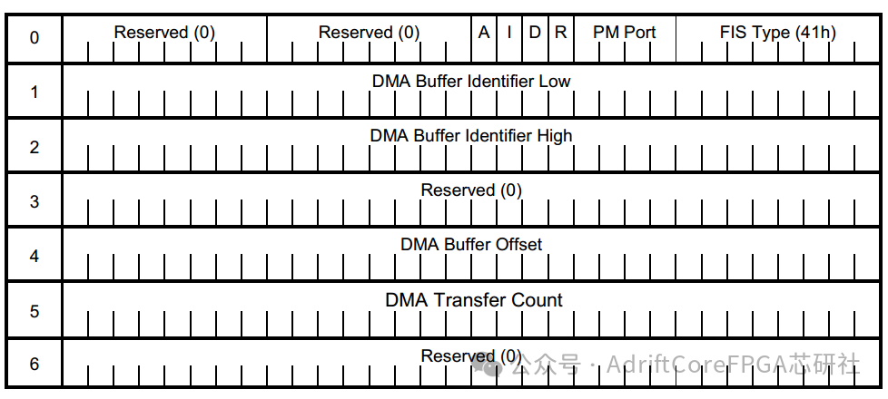
All DMA-based data transfers (including NCQ) rely on it to establish the DMA context
What is its purpose?
- • It is a FIS that can be sent in both directions (Host ↔ Device) (hence the name includes both “Host to Device” and “Device to Host”).
- • Its role is to: inform the receiver how to configure the DMA controller (DMA buffer id, offset, transfer length, direction, etc.), thus preparing for subsequent data transfers.
In other words: Without DMA Setup FIS, neither the Host nor the Device knows “where the data should be placed in memory”, “how many bytes to transfer”, or “the direction of the transfer”.
Field analysis
- • FIS Type = 41h: Uniquely identifies it as DMA Setup FIS, with a total length of 7 Dwords (fixed length).
- • D (Direction):
- •
<span>1 = transmitter → receiver</span>(e.g., Device sends data to Host). - •
<span>0 = receiver → transmitter</span>(e.g., Host writes data to Device). - • A (Auto-Activate):
- •
<span>1 = omit DMA Activate FIS</span>, start data transfer directly (optimized mode). - •
<span>0 = requires DMA Activate FIS</span>to trigger data transfer (safer, default mode). - • DMA Buffer Identifier (Low/High):
- • A “buffer descriptor” provided by the Host.
- • It may be a physical address or a more complex SG List (scatter-gather list).
- • Its role is to inform the other party where the data should be stored in memory.
- • DMA Buffer Offset: The offset of the data in the buffer (byte-aligned to 4 bytes).
- • DMA Transfer Count: The number of bytes to be transferred (low bit aligned).
- • I (Interrupt):
- •
<span>1 = trigger interrupt upon transfer completion</span>. - • Usually not enabled during user data transfers, but will be used during command/status transfers.
- • PM Port: Used when going through a Port Multiplier, directly connected hard drives are
<span>0</span>. - • Reserved: Must be cleared to zero.
Workflow
Here is a typical DMA write (Host → Device) example:
- 1. Host sends DMA Setup FIS: Telling the Device, “I want to write 128KB to you, starting from memory address X”.
- 2. Device configures the DMA controller, preparing to receive data.
- 3.
* If **A=0**: Device sends another **DMA Activate FIS** to the Host as a "gate opening signal".
* If **A=1**: Directly enter the data flow, no need for DMA Activate.- 4. Host sends Data FIS (with data).
- 5. Repeat Data FIS until Transfer Count is exhausted.
- 6. Finally, the Device informs the completion status using Register D2H FIS or Set Device Bits FIS.
For DMA read (Device → Host), it is similar, just the direction is reversed.
Significance of Auto-Activate
- • Normal mode (A=0):
- • Before each Host write, it must wait for the Device to send another DMA Activate FIS → an extra handshake.
- • Optimized mode (A=1):
- • After the Host sends DMA Setup FIS, it can immediately send Data FIS → one less round trip, improving efficiency.
- • However:
- • The Host must explicitly enable Auto-Activate (the switch mentioned in Section 13.3.2 of the protocol).
- • Otherwise, the Device is not allowed to use it casually, as the Host may not be ready.
Thus, Auto-Activate is a performance optimization feature, but it has compatibility requirements.
Design concept
- • SATA introduces DMA Setup FIS primarily for First-Party DMA:
- • Allowing the Host/Device to directly drive the DMA controller to read/write memory, rather than relying on the CPU for data transfer.
- • Crucial for performance and concurrency (especially NCQ).
- • It encapsulates Buffer Identifier + Offset + Count into the FIS, achieving an abstraction of memory areas.
- • As long as the context remains the same for each transfer, multiple Data FIS can be sent continuously without repeating the memory address description → improving bandwidth utilization.
PIO-Setup
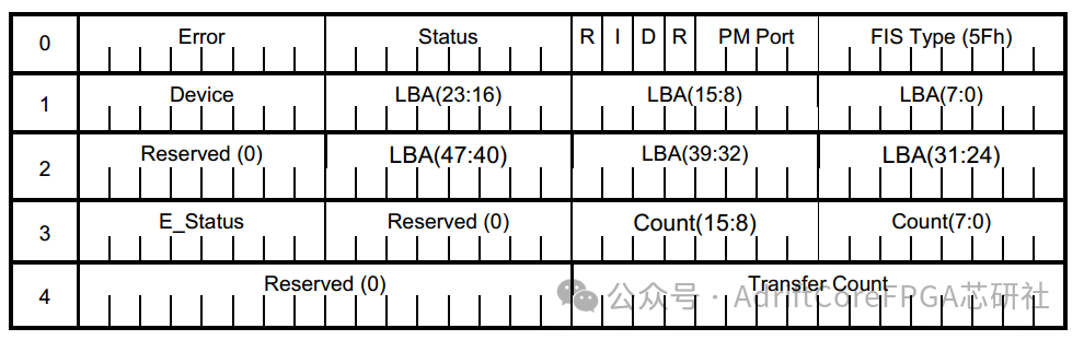
A frame specifically used in the SATA protocol to support PIO (Programmed I/O) data transfer.
Basic information
- • FIS Type: 5Fh, a fixed value indicating this is a PIO Setup FIS.
- • Length: 5 Dwords (20 bytes).
- • Fields: Mainly include LBA address, Device registers, Status/Error, Count registers, Transfer Count, etc.
- • D bit: Direction bit, determining whether data is Device → Host or Host → Device.
- • I bit: Interrupt bit, indicating whether to trigger an interrupt after the transfer is complete.
Design purpose
In PIO mode, data transfer involves active participation from the CPU, which is slower and has strict timing requirements. Therefore, SATA defines the PIO Setup FIS to inform the Host how to prepare for an upcoming data transfer before the actual data is transmitted.
Key points:
- • Before each PIO data transfer, the Device must first send a PIO Setup FIS.
- • It provides initial status (Status), final status (E_Status), error register (Error), transfer length (Transfer Count), etc.
- • The Host uses this information to arrange CPU access to shadow registers for data transfer.
Transfer scenarios
Host → Device (Write scenario)
- 1. The Device first sends a PIO Setup FIS, informing the Host how much data to write and what the initial/final statuses are.
- 2. Upon receiving it, the Host:
- • Updates the shadow registers.
- • Loads the Transfer Length into the countdown register.
- • The CPU writes data into the Data Register word by word → HBA assembles it into Data FIS to send to the Device.
- • At the end of the transfer, it writes the E_Status back to Shadow Status (must be completed within 400ns).
Device → Host (Read scenario)
- 1. The Device first sends a PIO Setup FIS, informing the Host: I am ready to send data, and the transfer length is how much.
- 2. Upon receiving it, the Host:
- • Saves Status/Error/E_Status.
- • Loads Transfer Length.
- • Waits for the Device to send Data FIS.
- • The Host reads from the Data Register, decrementing the countdown register.
- • When the transfer is complete, it writes the E_Status back to Shadow Status (within 400ns).
Why are two statuses (Status and E_Status) needed?
The timing in PIO mode is quite “rigid”:
- • At the start: The Host needs to know that the Device has cleared BSY and set DRQ → indicating that the Device is ready with data.
- • At the end: The Host needs to know that the Device has cleared DRQ and possibly reset BSY → indicating that the Device has completed processing.
Therefore, the PIO Setup FIS provides both initial status (Status) and final status (E_Status), allowing the Host to accurately simulate the traditional ATA handshake process.
Summary
- • PIO Setup – Device to Host FIS is the “preparation frame” for PIO transfers.
- • It is sent by the Device, informing the Host how many bytes will be transferred, the data direction, initial/final statuses, and other information.
- • The Host uses it to update shadow registers and drive the CPU to perform the actual data transfer (Data FIS).
- • Each PIO data transfer requires such an FIS.
- • Its role is to simulate the strict timing requirements of traditional ATA in the SATA protocol, ensuring compatibility.
Data
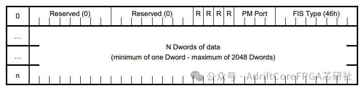
What is its purpose?
It is the “truck” for moving data.
- • Host → Device: Writing data to the hard drive (writing sectors).
- • Device → Host: Reading data to the host (reading sectors).
It does not carry commands or statuses, only responsible for packaging and transmitting data.
When is this FIS sent?
- • In PIO mode: After PIO Setup FIS → followed by Data FIS.
- • In DMA mode: After DMA Setup / DMA Activate → starts sending Data FIS.
- • In First-party DMA: The Device also uses Data FIS to load data into the host memory.
How is data packed inside?
- • In units of Dword (4 bytes).
- • If the data is not a multiple of 4, the last Dword is padded with 0.
- • A maximum of 2048 Dwords = 8192 bytes = 16 sectors can be packed at once. If it exceeds 8KB, it must be split into multiple Data FIS for transmission.
How does it know how much data to transmit?
The Data FIS itself does not carry a “length field”. The length comes from the previous context FIS:
- • If it is PIO, refer to the Transfer Count in the PIO Setup FIS.
- • If it is DMA, refer to the previous DMA Setup / Activate FIS.
The receiver confirms how much data was actually received by counting Dwords (between SOFP and EOFP).
Special rules
- • SATA does not support legendary byte counts (must be word granularity, 2 bytes).
- • If it is an odd number of words (e.g., 3 words = 6 bytes):
- • The last word is placed in the low 16 bits of the Dword, with the high 16 bits padded with zeros.
How does the receiver process it?
- • It does not wait for the entire FIS to be received before checking CRC, but rather processes it as it receives.
- • If the CRC is incorrect, the error will be reported in the command completion status, not in the Data FIS.
Data transfer process
PIO (Programmed I/O) data transfer process
In PIO mode, the CPU directly participates in data transfer, with data transmitted through register windows between the Host and Device.
- 1. Host initiates a command
- • The Host writes to the Command Register (Command FIS), such as READ SECTORS or WRITE SECTORS.
- • The Device enters BSY=1, preparing to process the command.
- • The Device notifies the Host through PIO Setup FIS:
- • The direction of read or write (D→H or H→D).
- • The number of bytes to be transferred (up to one sector or several sectors).
- • Related status/error codes.
- • If it is PIO-IN (read): The Device places data in the Data Register, and the Host polls or triggers reading via interrupt.
- • If it is PIO-OUT (write): The Host writes data into the Data Register, and the Device retrieves it.
- • This process requires the CPU to loop read/write registers, which is inefficient.
- • After a data block transfer is completed, the Device updates the Status and may send another PIO Setup FIS (if there is more data to transfer).
- • Finally, the Device sends Set Device Bit FIS or indicates command completion through Status=DRDY.
Scenario: Small data volumes, compatibility, and low-speed devices. Typically used in early IDE modes, now mostly seen in initialization/debugging.
DMA (Direct Memory Access) data transfer process
In DMA mode, data is directly transferred between Host memory and Device, without the CPU participating byte by byte.
- 1. Host initiates a command
- • The Host writes to the Command Register (Command FIS), such as READ DMA EXT or WRITE DMA EXT.
- • At the same time, it prepares the memory buffer in the PRD (Physical Region Descriptor Table).
- • The Device sends DMA Setup FIS, informing the Host:
- • The direction (read/write).
- • The length of data to be transferred.
- • The Ready signal, indicating it is ready to start DMA.
- • After the Host receives the DMA Setup FIS, it triggers the DMA Engine.
- • The Device sends DMA Activate FIS, confirming that the transfer can officially begin.
- • Data is rapidly transferred via SATA Data FIS between the HBA (Host Bus Adapter) and Device, directly writing into memory.
- • After the Device completes the transfer, it sends Set Device Bit FIS / D2H Register FIS to notify the Host.
- • The Host releases resources, and the command is completed.
Scenario: Large data volumes (e.g., reading/writing disks), high throughput, and when CPU load needs to be reduced, almost all modern storage devices use DMA.
Brief Comparison
- • PIO: Data is moved through the CPU via registers → memory, low efficiency but simple logic.
- • DMA: Data bypasses the CPU, directly between memory ↔ Device, efficient and supports high bandwidth.
- • FIS links:
- • PIO →
<span>PIO Setup FIS</span>+<span>Data FIS</span> - • DMA →
<span>DMA Setup FIS</span>→<span>DMA Activate FIS</span>→<span>Data FIS</span>
Final Thoughts
It can be said that the FIS mechanism of SATA breaks down complex data transfers into a rhythmic closed loop of configuration → authorization → transfer → completion. Understanding the roles and interaction logic of these FIS will clarify the trade-offs of reliability and compatibility in the design of the SATA protocol, and help avoid detours during debugging and implementation.
Previous Issues Review
SATA Protocol Series
Learn a bit every day to integrate SystemVerilog syntax (collection)
Other technical columns
Appendix A
Welcome to join the FPGA/IC exclusive AI knowledge base, where you can access more knowledge without downloading an app, just use the WeChat mini-program for one-click access.
Click the link to join
Appendix B
Welcome to join the FPGA and digital IC learning group! Here, you can ask questions, share your learning experiences, or participate in interesting discussions.
Link: FPGA Chip Research Society
#FPGA #Digital IC #SATA Protocol #FIS Frame Information Structure #Transport Layer Design #Link Layer Communication #Shadow Register Block #Storage Device Communication Protocol #SATA3 Specification #ATA8ACS Standard #In-depth Analysis of Storage Protocols #Storage Technology Essentials #Essential for Hardware Engineers #Protocol Layer Explanation