When performing SMT (Surface Mount Technology) processing on PCBs, the PCBs are conveyed along the SMT production line via guide rails. Therefore, a pair of edges must be reserved as forbidden areas for component placement. Typically, the two long edges of the PCB or the assembled panel are designated as the conveyance edges.
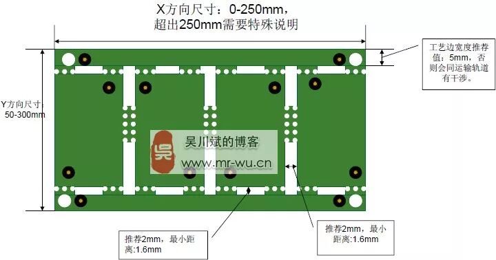
The width of the SMT conveyor rail fixed plate is 3.0mm. The theoretical limit for the conveyance edge is 3.0mm, but it is recommended not to reach this limit as it increases the difficulty of component placement. It is advisable to leave some extra space as a margin, with 5.0mm suggested as the conveyance edge’s “forbidden area”.
If this forbidden area margin is insufficient, the interference portion will affect the solder paste or already placed components once the PCB is on the conveyor rail. The edges of the board that are interfered with can only be re-soldered or require additional fixtures, increasing production costs.
If the surface-mounted components on the board are far enough from the edges and do not fall within the track range, no additional process edges are needed. However, if components are within the track range, process edges must be added as clamping areas. The width of the process edge depends on the machine characteristics, typically requiring 3-10mm, with 5mm being the most common.

Generally, process edges are added to the longer side of the board, with the board entering the SMT machine vertically. This orientation provides higher rigidity, preventing the board from bouncing due to the slight pressure of the machine’s probe during placement. However, adding process edges to the longer side increases the area, indirectly raising the average price per board. If the board’s rigidity is sufficient, process edges can be added to the shorter direction, reducing the area and lowering the average cost per board, with the board entering the SMT machine horizontally.
SMT typically uses MARK points for alignment. If there are no MARK points on the board, 2-4 MARK points must be added diagonally on the process edge. The size of the MARK points is generally 1.0mm, with exposed copper for soldering. If there are existing MARK points on the board, the addition of process edges is optional.
During production, the board factory requires positioning for forming and testing. Special positioning holes are added to the process edges to create a relatively standard shape, making positioning easier. Therefore, 3-4 positioning holes with diameters between 2.0-4.0mm are added, with 3mm being the most common and preferred size.
Here are some design considerations for process edges:
-
Components for surface mount or through-hole insertion cannot be arranged within the process edge, and their physical presence must not extend into the process edge or above it.
-
The physical presence of hand-inserted components must not fall within 3mm above the upper and lower process edges, or within 2mm above the left and right process edges.
-
The conductive copper foil within the process edge should be as wide as possible. Lines smaller than 0.4mm require enhanced insulation and wear resistance treatment, while the outermost lines should not be less than 0.8mm.
-
The process edge can be connected to the PCB using stamp holes or V-shaped grooves, with V-shaped grooves generally preferred.
-
There should be no pads or through-holes on the process edge.
-
For single boards larger than 80 mm², the PCB must have a pair of mutually parallel process edges, and no component presence is allowed in the space above and below the process edges.
-
The width of the process edge can be increased appropriately based on actual conditions.