Nowadays, the rapid prototyping of PCBs is incredibly convenient. By placing orders through online platforms, you can receive PCB samples without having to interact with factory personnel.
However, if you are not familiar with the PCB production process, some quality issues caused by your own design may lead to misunderstandings during communication with the factory’s technical staff, making you feel like the factory is trying to take advantage of you, which can be quite frustrating 😂
For example:
You hurriedly submitted your PCB photolithography files for prototyping before the factory’s order review closed at 6 PM. Later that evening, feeling uneasy, you checked the PCB design files again and found a small issue with the photolithography files. The next morning, you rushed to contact the factory to cancel the order, but they said the photolithography had already been processed and could not be changed!
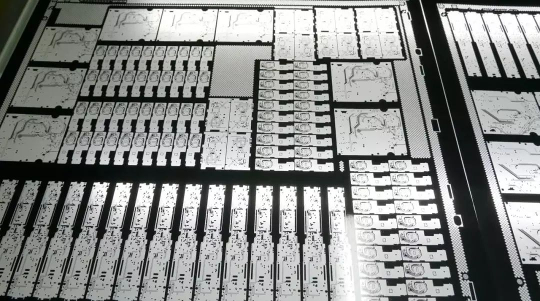
Why can’t it be modified? Through the PCB factory videos, you will understand that your prototyping files are combined with others’ design files to produce the film. If modifications are made, the entire scheduling of the factory will be disrupted.
Another example:
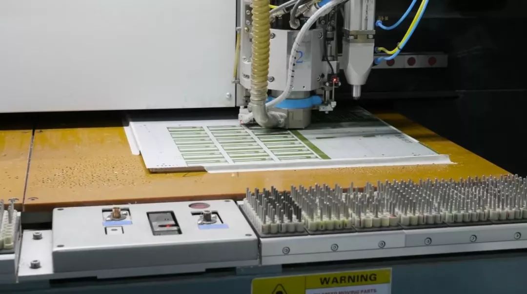
Why does the factory charge extra for drilling when you have filled the PCB with vias?
Through the videos, you can learn that during the drilling process, mechanical holes on the PCB are drilled one by one. If there are too many vias, the drilling time increases, leading to greater wear on the drill bits. If the spacing between vias is smaller than the drill’s capability, either production cannot proceed, or laser drilling must be used, resulting in a significant price increase.
Old Wu believes that PCB design engineers should understand the factory’s technical capabilities and manufacturing processes. However, not everyone has the opportunity to visit a factory to learn about it. Therefore, Old Wu shares some factory visit videos on his blog.
In 2015, Old Wu was invited to visit the PCB factory of Jingwang located in Shenzhen. Shenzhen Jingwang Electronics Co., Ltd. is one of the top 100 PCB factories in China, and its manufacturing processes are relatively advanced.
Old Wu shared some discussion and exchange videos from his visit to Jingwang, which you can find in this article on Old Wu’s blog:
【It’s time to visit a PCB factory!】
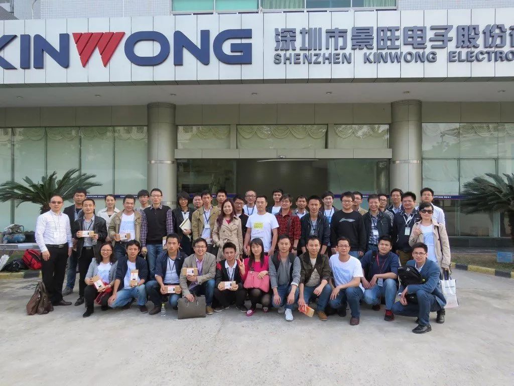
Blog link:https://www.mr-wu.cn/shi-shi-hou-qu-pcb-ban-chang-lang-yi-bo-le/
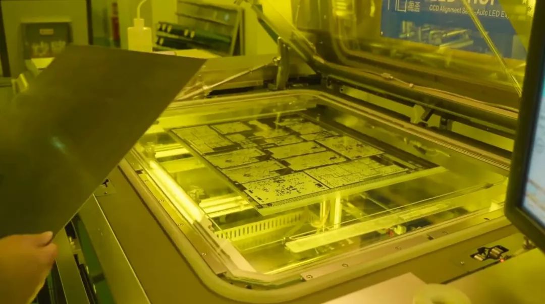
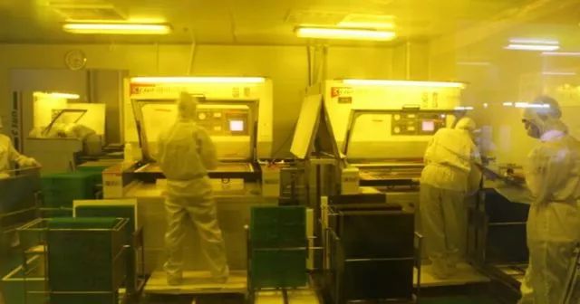
Another article on Old Wu’s blog features a promotional video of the production line at EURO CIRCUITS factory, from which we can learn about the entire production process from Gerber files to finished PCBs.
【Introduction to PCB Factory Production Process】
Blog link:https://www.mr-wu.cn/video-for-pcb-production-process/
The two articles above feature mid to high-end factories. For a representative video of an economical and practical quick PCB factory, you can refer to Old Wu’s article:
【Shenzhen Jialichuang PCB Factory Visit Video】
Blog link: https://www.mr-wu.cn/shen-zhen-jia-li-chuang-pcb-ban-chang-can-guan-shi-pin/