Engineering A-Site NaNbO₃ Lead-Free Antiferroelectrics Achieve Distinct Double Hysteresis Loops

Engineering A-Site NaNbO₃ Lead-Free Antiferroelectrics Achieve Distinct Double Hysteresis Loops

Title J Am Ceram Soc:Engineering A-Site NaNbO₃ Lead-Free Antiferroelectrics Achieve Distinct Double Hysteresis Loops Material System: (Na₁–₂ₓ-yCaₓAgᵧ)NbO₃ (100xCa-100yAg) Ceramics Research Background Antiferroelectrics (AFEs) have significant applications in energy storage capacitors due to their unique double hysteresis loop characteristics. Traditional PbZrO₃-based materials pose environmental hazards, while NaNbO₃ (NN) faces irreversible challenges in AFE-FE phase transitions as … Read more
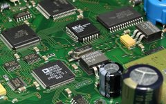
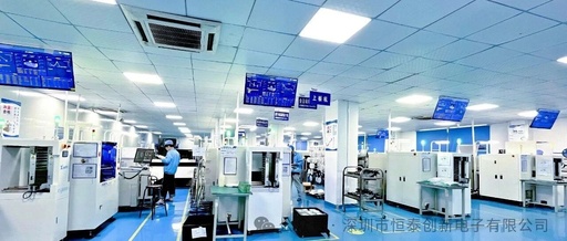
Criteria for Selecting Surface Treatment Processes in PCB Manufacturing

Criteria for Selecting Surface Treatment Processes in PCB Manufacturing

The most basic purpose of PCB surface treatment is to ensure good solderability or electrical performance.Since copper in nature tends to exist in the form of oxides in the air, it is unlikely to remain as pure copper for a long time, so additional treatments are required for copper.There are now many PCB surface treatment … Read more

Choosing Between Lead and Lead-Free PCBA Processes: Why Lead-Free Dominates and What Supports Lead-Based?

Choosing Between Lead and Lead-Free PCBA Processes: Why Lead-Free Dominates and What Supports Lead-Based?

Why Use Lead-Free PCBA Lead-free processes use environmentally friendly solder, aligning with modern green trends. Lead is a toxic heavy metal, and prolonged exposure to lead-containing materials can pose potential health risks to operators, while the disposal of lead waste can also pollute the environment. Additionally, lead-free solder has a higher melting point, typically between … Read more