Many students learning embedded systems often feel confused by various protocols and can’t distinguish their functions. Today, I will clarify the five commonly used protocols in embedded systems, packed with useful information. Without further ado, let’s get started!
UART Communication Protocol
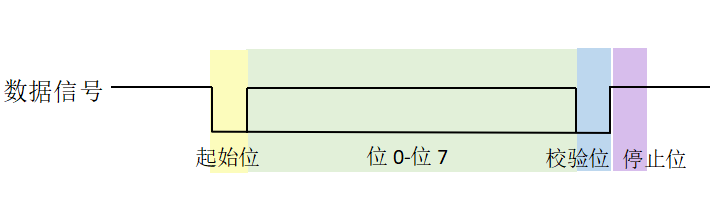
The data packet in serial communication is transmitted from the sending device through its TXD interface to the receiving device’s RXD interface. In the protocol layer of serial communication, the content of the data packet is defined, consisting of a start bit, main data, a parity bit, and a stop bit. Both parties must agree on the data packet format to successfully send and receive data.
This discussion primarily focuses on asynchronous serial communication. In asynchronous communication, since there is no clock signal, both communicating devices must agree on the baud rate, which is the length of each symbol, to decode the signals. Each segment separated by dashed lines in the above image represents one symbol. Common baud rates include 4800, 9600, and 115200.
3. Start and Stop Signals
A data packet in serial communication begins with a start signal and ends with a stop signal. The start signal of the data packet is represented by a logical 0 bit, while the stop signal can be represented by 0.5, 1, 1.5, or 2 logical 1 bits, as long as both parties agree.
Immediately following the start bit is the main data content to be transmitted, also known as valid data. The length of valid data is often agreed to be 5, 6, 7, or 8 bits long.
After the valid data, there is an optional parity bit. Since data communication is relatively susceptible to external interference, leading to transmission errors, a parity bit can be added during the transmission process to address this issue. Parity methods include odd parity, even parity, space parity, mark parity, and no parity.
-
Odd Parity requires the total number of “1” bits in the valid data and parity bit to be odd. For example, if an 8-bit valid data is: 01101001, which has 4 “1” bits, to achieve odd parity, the parity bit would be “1”, resulting in a total of 9 bits for transmission.
-
Even Parity is the opposite of odd parity, requiring the total number of “1” bits in the frame data and parity bit to be even. For instance, if the data frame is: 11001010, which has 4 “1” bits, the even parity bit would be “0”.
-
Space Parity sets the parity bit to always be “0” irrespective of the valid data.
-
Mark Parity sets the parity bit to always be “1”.
-
In the case of no parity, the data packet does not include a parity bit.
IIC Communication Protocol
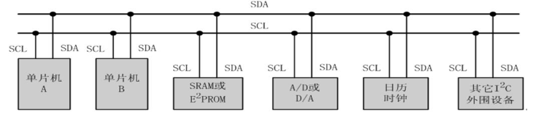
I2C, short for Inter-Integrated Circuit, is pronounced I-squared-C. It was proposed by Philips in the 1980s to allow motherboards, embedded systems, or mobile phones to connect to low-speed peripheral devices. Its main use is for communication between SOC and peripheral devices (such as EEPROMs, capacitive touch chips, various sensors, etc.).
The I2C bus uses only two bidirectional open-drain signal lines (serial data line: SDA, and serial clock line: SCL), utilizing pull-up resistors.
-
SCL (Serial Clock): The serial clock line transmits the CLK signal, usually provided by the master device;
-
SDA (Serial Data): The serial data line transmits communication data. I2C uses a 7-bit device address, allowing a maximum of 112 nodes to communicate on one bus. The maximum communication number is limited by the address space and a total bus capacitance of 400pF.
The I2C bus is widely used in interfaces for EEPROMs, real-time clocks, LCDs, and other chips.
The I2C protocol allows for a considerable operating voltage range, with typical voltage references of +3.3V or +5V.
Common I2C buses are categorized into different modes based on transmission rates: standard mode (100Kbit/s), low-speed mode (10Kbit/s), fast mode (400Kbit/s), and high-speed mode (3.4Mbit/s). The clock frequency can be reduced to zero, effectively pausing communication. This bus is a multi-master bus, meaning multiple master device nodes can be placed on the bus. After the stop bit (P) is issued, indicating the end of communication, the master device node can become a slave device node.
Master Device Node: The device node that generates the clock and initiates communication.
Slave Device Node: The device node that receives the clock and responds to the master device’s addressing.
(1) In I2C communication, the roles of the two parties are not equal. Communication is initiated by the master device, which dominates the transmission process. The slave device receives the data sent by the master device according to the I2C protocol and responds in a timely manner.
(2) The roles of the master and slave devices are determined by the communicating parties (the I2C protocol itself does not specify); either can act as a master or slave (software configuration is required).
(3) The master device is responsible for scheduling the bus and deciding which slave device to communicate with at any given time. At the same time, only one pair of master and slave devices can communicate on the I2C bus.
(4) Each I2C slave device has a unique I2C slave address, which is an inherent property of the slave device. During communication, the master device uses the slave address to locate the slave device.
Idle State: No devices are communicating.
Busy State: One slave device and the master device are communicating, occupying the I2C bus, while other slave devices are in a waiting state.
4. Communication Protocol
Timing: Timing in communication refers to the sequential changes in levels on the communication line and the significance of these changes for communication.
Each communication cycle begins with a start bit and ends with a stop bit, with the data being transmitted in between.
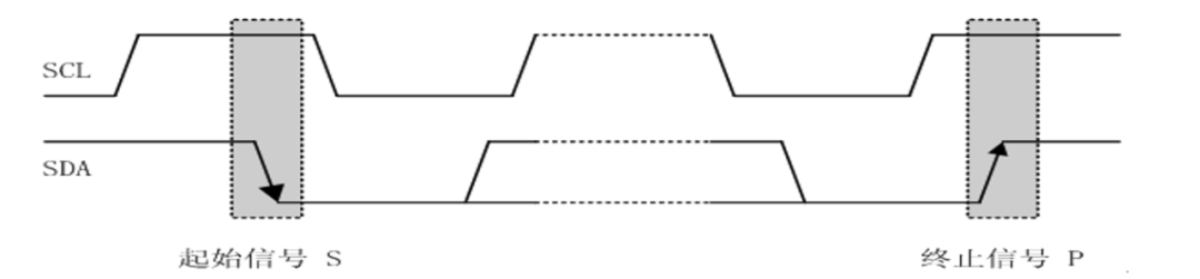
I2C communication begins with a start bit and ends with a stop bit, releasing the I2C bus. Both the start and stop bits are issued by the master device.
Start Bit (S): When SCL is high, SDA transitions from high to low.
Stop Bit (P): When SCL is high, SDA transitions from low to high.
4.2 Data Format and Acknowledgment
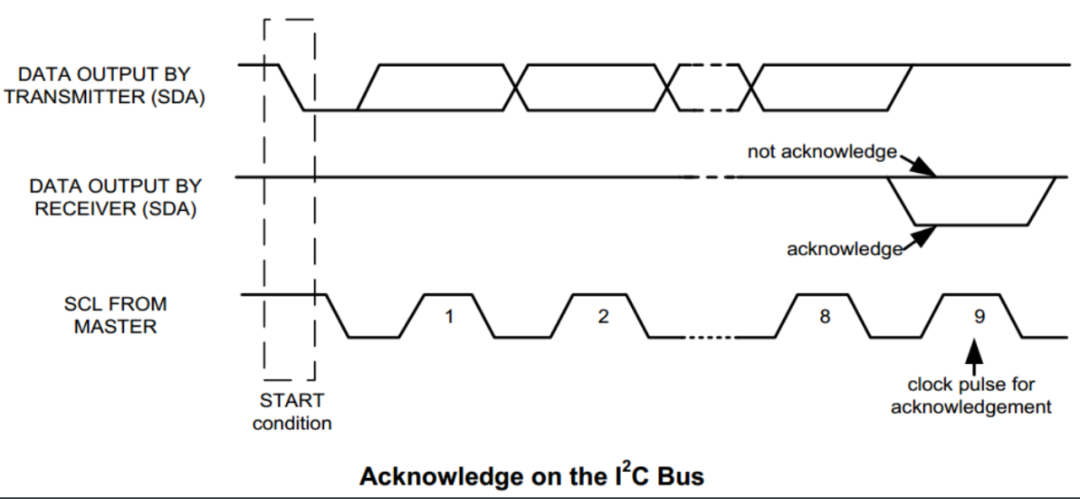
I2C data is transmitted in bytes (i.e., 8 bits). After each byte is transmitted, there will be an ACK acknowledgment signal. The acknowledgment signal’s clock is generated by the master device.
Acknowledgment (ACK): Pull down the SDA line and keep it low while SCL is high.
No Acknowledgment (NOACK): Do not pull down the SDA line (the SDA line remains high), and keep the SDA line high while SCL is high.
During transmission, if the slave device cannot process the data sent by the master device in time, it will hold the SCL line low, forcing the master device to wait until the slave device releases the SCL line, after which data transmission can resume.
5. Data Transmission Communication
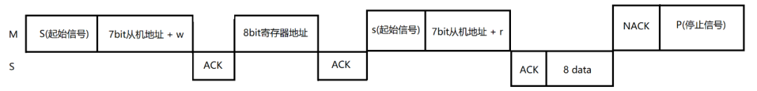
After starting data transmission, a start bit (S) is sent, followed by the master device sending an address. The master device then releases the SDA line and waits for the slave device’s acknowledgment signal (ACK). Each byte of data transmission must be followed by an acknowledgment signal bit. Data transmission ends with a stop bit (P), releasing the I2C bus.
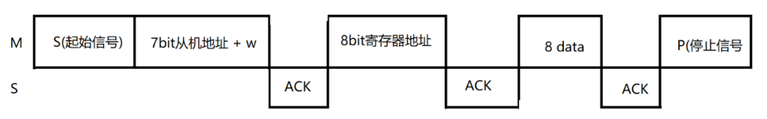
When communication starts, the master device first sends a start signal (S), followed by sending an address. The master device then releases the SDA line and waits for the slave device’s acknowledgment signal (ACK). After the slave device acknowledges the master device, the master device sends the register address to read, and the slave device acknowledges (ACK). The master device then sends a repeated start signal (Sr), followed by the device address (including the read flag), the slave device acknowledges the master device, and sends the value of the register to the master device.
SPI Communication Protocol
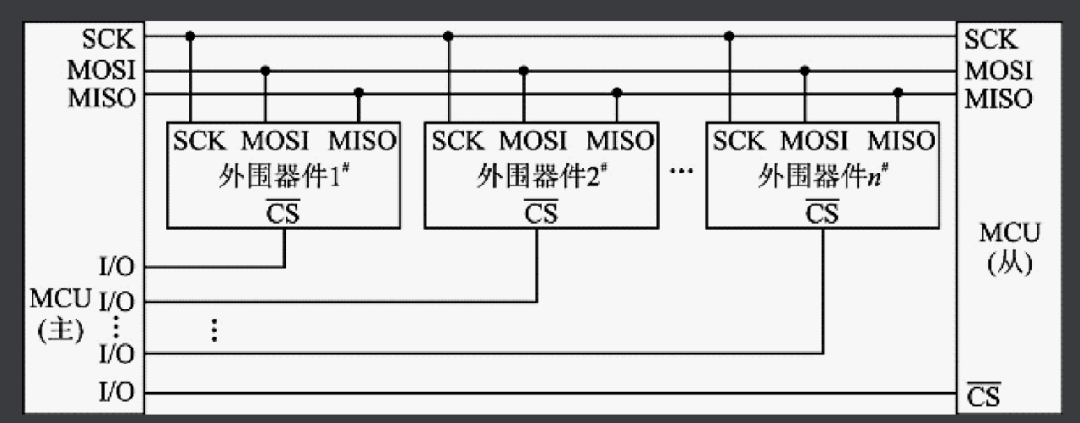
The SPI interface is a full-duplex synchronous serial bus first proposed by Motorola, using a master-slave architecture that supports multi-slave mode applications.
In practical development, most designs use a single master. In multi-slave mode, the clock is controlled by the master. Data is transmitted bit by bit under clock shift pulses, with high bits first or low bits first.
The SPI interface has two unidirectional data lines for full-duplex communication, with current data rates in applications reaching several Mbps.
2. SPI Bus Hardware Connections
-
Device Selection Line: NSS
-
-
Serial Output Data Line: MOSI
-
Serial Input Data Line: MISO
M: master O: output S: slave I: input
(1) MOSI: Master device data output (write), slave device data input (read)
(2) MISO: Master device data input, slave device data output
(3) SCLK: Clock signal generated by the master device
(4) /SS: Slave device enable signal controlled by the master device (chip select line)
Supports full-duplex communication, simple communication, and fast data transmission rates.
There is no specified flow control, and no acknowledgment mechanism to confirm whether data has been received, resulting in some reliability issues when compared to the IIC bus protocol.
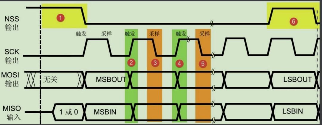
5. Detailed Explanation of Protocol Communication Timing
-
Start Signal: The NSS signal line transitions from high to low, marking the start of SPI communication.
-
End Signal:The NSS signal transitions from low to high, marking the end of SPI communication.
-
Data Transmission:SPI uses the MOSI and MISO signal lines to transmit data, synchronizing data using the SCK signal line. Data is transmitted bit by bit during each clock cycle of SCK, with input and output occurring simultaneously. SPI can transmit data in 8 or 16-bit units, with no limit on the number of units transmitted at once.
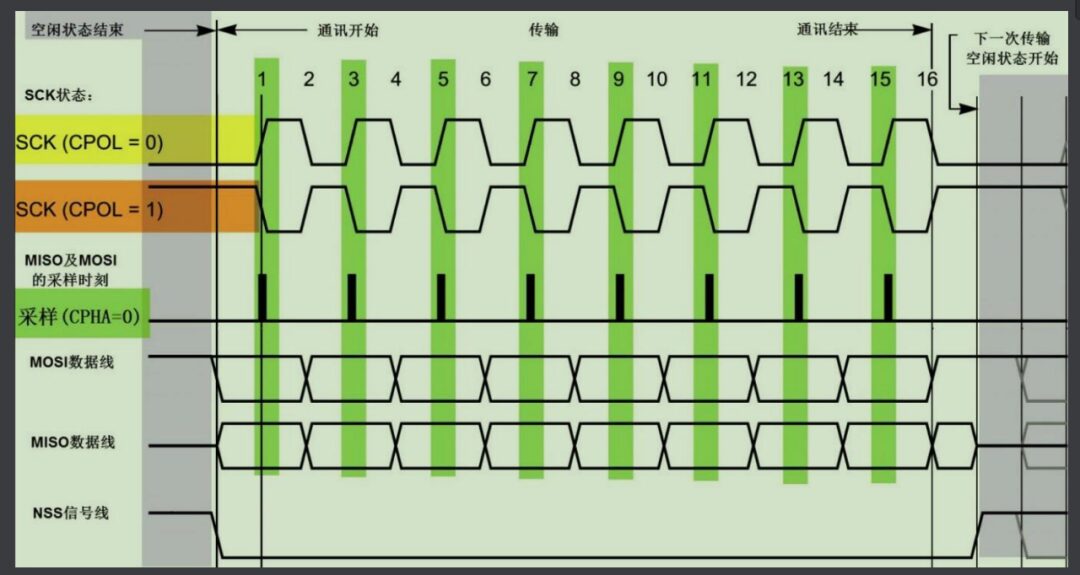
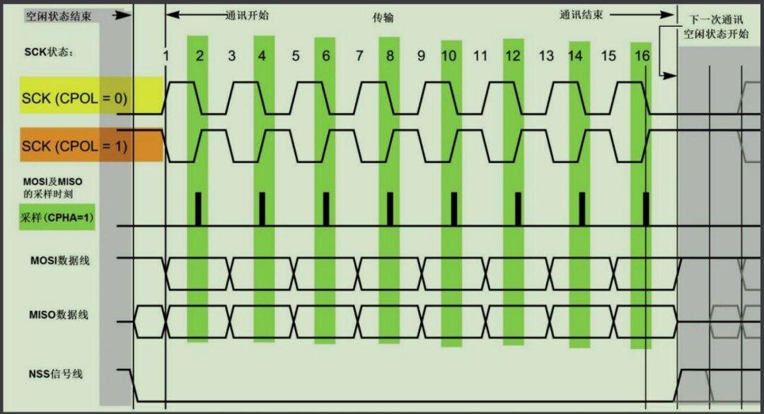
6. SPI Bus Communication Modes

The RS-232 interface complies with the serial data communication interface standard established by the Electronic Industries Alliance (EIA). The original designation is EIA-RS-232 (commonly referred to as RS232), and it is widely used for connecting serial interface peripherals to computers, including connection cables, mechanical, electrical, signal, and transmission processes. The RS-232-C standard specifies data transmission rates of 50, 75, 100, 150, 300, 600, 1200, 2400, 4800, 9600, and 19200 baud.
RS-232 is one of the mainstream serial communication interfaces today. Due to the early emergence of the RS232 interface standard, it inevitably has some shortcomings, primarily four points:
(1) The signal level values of the interface are relatively high, making it easy to damage the interface circuit’s chips. The voltage of any signal line in RS232 is in a negative logic relationship. That is, logic “1” is -3V to -15V; logic “0” is +3V to +15V, with a noise tolerance of 2V. This means the receiver must recognize signals above +3V as logic “0” and below -3V as logic “1”. TTL levels of 5V are positive logic, while 0 is negative logic. They are not compatible with TTL levels, hence a level conversion circuit is required to connect with TTL circuits.
(2) Low transmission rates, with a bit rate of 20Kbps during asynchronous transmission; hence, in the 51CPLD development board, the baud rate can only be set to 19200 for this reason.
(3) The interface uses one signal line and one return signal line to form a common-ground transmission format, which is prone to common-mode interference, thus exhibiting weak noise immunity.
(4) Limited transmission distance. The maximum standard transmission distance is 50 feet, practically it can only be used within about 15 meters.
RS-485 serial bus is widely used when communication distances are required to be several dozen meters to thousands of meters. RS-485 uses balanced transmission and differential reception, thus having the ability to suppress common-mode interference. Additionally, the bus transceiver has high sensitivity, capable of detecting voltages as low as 200mV, allowing the transmitted signals to be recovered over long distances. RS-485 operates in half-duplex mode, meaning that only one point can be in transmission state at any given time; therefore, the transmission circuit must be controlled by an enable signal.
RS-485 is very convenient for multipoint interconnection, allowing for the elimination of many signal lines. Using RS-485 can create a distributed system that allows for up to 32 drivers and 32 receivers connected in parallel. In response to the shortcomings of RS-232-C, the new standard RS-485 has the following features:
(1) The electrical characteristics of RS-485: logic “1” is represented by a voltage difference of +2V to +6V between the two wires, and logic “0” is represented by a voltage difference of -6V to -2V. The signal levels of the interface are lower than those of RS-232-C, making it less likely to damage the interface circuit chips, and this level is compatible with TTL levels, facilitating connection with TTL circuits.
(2) The maximum data transmission rate is 10Mbps.
(3) The RS-485 interface uses a combination of balanced drivers and differential receivers, providing strong common-mode interference immunity, thus exhibiting good noise performance.
(4) The maximum transmission distance is standardized at 4000 feet, practically reaching 3000 meters.
(5) The RS-232-C interface only allows for one transceiver connection on the bus, meaning it has single-station capability; in contrast, the RS-485 interface allows for the connection of up to 128 transceivers on the bus, providing multi-station capability, which allows users to conveniently establish a device network using a single RS-485 interface.
Comparison between IIC and SPI Buses
Both use serial synchronous buses, both use TTL levels, and both employ a master-slave architecture.
-
The IIC bus is half-duplex communication, as it only has one SDA data line.
-
The SPI bus is full-duplex communication, as it has two unidirectional data lines (MOSI and MISO).
-
The IIC bus has acknowledgment signals, while the SPI bus does not.
-
The IIC bus selects which slave device to communicate with through addressing.
-
The SPI bus selects which slave device to communicate with through chip select lines, sending enable signals to the slave devices.
-
For example, if there are 10 slave devices, 10 chip select lines are needed, which can waste hardware pin resources.
-
The IIC bus transmits data through high and low level changes.
-
The SPI bus samples data on the edge trigger.
Comparison between RS232 and RS485 Buses
Working Modes: RS232 is full-duplex, while RS485 is half-duplex.
Transmission Methods: RS485 and RS232 are merely the physical protocol of communication (i.e., interface standards); RS485 is differential transmission, while RS232 is single-ended transmission, but the communication programs are not significantly different.
Signal Lines: The RS485 interface forms a half-duplex network that typically requires only two signal lines. The RS-232 interface generally uses three lines: RXD, TXD, and GND.
Interference Immunity: The RS485 interface uses a combination of balanced drivers and differential receivers, exhibiting good noise immunity. The RS232 interface uses one signal line and one return signal line to form a common-ground transmission format, which is prone to common-mode interference.
Transmission Distance: The maximum standard transmission distance for the RS485 interface is 1200 meters (at 9600bps), while RS232 has a limited maximum transmission distance of 50 meters, practically being usable only within about 15 meters.
Communication Capability: The RS485 interface allows for the connection of up to 128 transceivers on the bus, enabling users to conveniently establish a device network using a single RS485 interface. RS232 only allows for one-to-one communication.
Transmission Rates: RS232 has a relatively low transmission rate, with a baud rate of 20Kbps during asynchronous transmission. RS485’s maximum data transmission rate is 10Mbps.
Electrical Level Values: In RS485, logic “1” is represented by a voltage difference of +(2-6)V between the two lines; logic “0” is represented by a voltage difference of -(2-6)V. In RS232, any signal line’s voltage is in a negative logic relationship, meaning: logic “1” is -(5-15)V; logic “0” is +(5-15)V.
What other embedded difficulties do you have?
Welcome to comment and leave messages to me!
I look forward to your messages!

Recommended Previous Articles
Super Useful! | What is Embedded CAN Bus?
Super Useful!| What are the Basic Principles of Embedded ARM?
985 Graduates Escape Employment Pressure, Sparking a Trend of Extended Graduation!
May Employment Trends| Average Salary 1W+! Highest Salary 18K! Employment Rate Reaches 99.99%!