
Click on the arrow
“blue text”
, follow us!
Q: How can I see such articles every day?
A: Just search for the public account “51 Microcontroller Learning Network” and follow for free.
This design guide discusses how to design RS-485 interface circuits. It covers the necessity of balanced transmission line standards and provides an example of process control design. The article also discusses line loading, signal attenuation, failure protection, and current isolation under separate headings.
1.Why Balanced Transmission Line Standards are Necessary
The focus of this article is on the most widely used balanced transmission line standard in industry: ANSI/TIA/EIA-485-A (hereinafter referred to as 485). After reviewing some key aspects of the 485 standard, it introduces how to implement differential transmission structures in practical projects through a factory automation example.
In long-distance, high-noise environments, data transmission between computer components and peripherals is often challenging. If possible, single-ended drivers and receivers should be used. For systems requiring long-distance communication, a balanced digital voltage interface is recommended.
485 is a balanced (differential) digital transmission line interface developed to improve the limitations of TIA/EIA-232 (hereinafter referred to as 232). The 485 standard has the following characteristics:
-
High communication rate – up to 50M bits/s
-
Long communication distance – up to 1200 meters (Note: at 100Kbps)
-
Differential transmission – lower noise radiation
-
Multiple drivers and receivers
In practical applications, if two or more computers require low-cost, reliable data communication, 485 drivers, receivers, or transceivers can be used. A typical example is the use of 485 to transmit information between a sales terminal and a central computer. Using twisted pair cables to transmit balanced signals has lower noise coupling, and since 485 has a wide common-mode voltage range, it allows communication rates of up to 50M bits/s or several kilometers at lower speeds.
Due to the widespread use of 485, more and more standard committees are adopting the 485 standard as the physical layer specification for their communication standards, including ANSI’s SCSI (Small Computer System Interface), Profibus standards, DIN measurement bus, and China’s multifunctional electric meter communication protocol standard DL/T645.
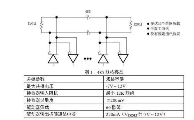
The balanced transmission line standard 485 was developed in 1983 for data transmission interfaces between hosts and peripherals. The standard only specifies the electrical layer; other aspects such as protocols, timing, serial or parallel data, and linkers are defined by the designer or higher-level protocols.
Initially, the 485 standard was defined as an upgrade in flexibility over the TIA/EIA-422 standard (hereinafter referred to as 422). Since 422 is only half-duplex communication (Note: 422 uses two pairs of differential communication lines, one pair for sending and one pair for receiving, so data is transmitted unidirectionally on one line), 485 allows multiple drivers and receivers on a single pair of signal lines, facilitating half-duplex communication (see Figure 1). Like 422, 485 does not specify a maximum cable length, but under 24-AWG cable and 100kbps conditions, it can transmit 1.2km; 485 also does not limit the maximum signal rate, which is instead limited by the rise time and bit time ratio, similar to 232. In most cases, due to transmission line effects and external noise, cable length is more likely to limit signal rates than the driver.
2.System Design Considerations
2.1 Line Loading
In the 485 standard, line loading must consider line termination and loads on the transmission line. Whether to match the transmission line termination depends on system design and is also influenced by transmission line length and signal rate (generally, low-speed short distances can be left without termination matching).
2.1.1 Transmission Line Termination Matching
Transmission lines can be divided into two models: distributed parameter model [1] and lumped parameter model [2]. Testing which model a transmission line belongs to depends on the signal transition (rise/fall) time tt and the propagation time from the driver output to the end of the cable tpd.
If 2tpd ≥ tt/5, the transmission line must be treated according to the distributed parameter model, and termination matching must be handled well; otherwise, the transmission line can be considered a lumped parameter model, in which case termination matching is not necessary.
Note 1: Distributed parameter model – the voltage and current in the circuit are functions of time and depend on the geometric size and spatial position of the devices.
Note 2: Lumped parameter model – the voltage between any two endpoints in the circuit and the current flowing into any device endpoint are completely determined, independent of the geometric size and spatial position of the devices.
2.1.2 Concept of Unit Load
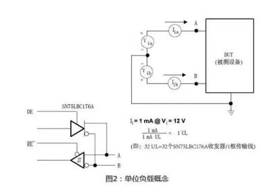
The maximum number of drivers and receivers connected to the same 485 communication bus depends on their load characteristics. The load of drivers and receivers is measured relative to a unit load. The 485 standard specifies that a maximum of 32 unit loads can be connected to a transmission bus.
Unit load is defined as: in a 12V common-mode voltage environment, allowing a steady-state load current of 1mA, or in a -7V common-mode voltage environment, allowing a steady-state load current of 0.8mA. Unit loads may consist of drivers, receivers, and failure protection resistors, but do not include AC termination matching resistors.
Figure 2 provides an example of unit load calculation for the SN75LBC176A transceiver. Since this device integrates the driver and receiver into a transceiver (i.e., the driver output and receiver input are connected to the same bus), it is difficult to separately obtain the driver leakage current and receiver input current. For calculation convenience, the receiver input impedance is considered to be 12 kΩ and a current of 1mA is given to the transceiver. This can represent one unit load, allowing 32 such loads on a transmission bus.
As long as the input impedance of the receiver is greater than 12kΩ, more than 32 such transceivers can be used on a single transmission bus.
2.2 Signal Attenuation and Distortion
A useful rule of thumb is that under maximum signal rate (in Hz) communication conditions, signal attenuation of -6dB is allowed. Generally, cable suppliers provide signal attenuation charts. The curve shown in Figure 3 illustrates the relationship between 24-AWG cable attenuation and frequency.
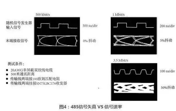
To determine the extent of random noise, jitter, distortion, etc., affecting the signal, the simplest method is to use an eye diagram. Figure 4 shows the signal distortion at the receiving end under different signal rates using 20AWG twisted pair cable at 500 meters. As the signal rate increases further, the impact of jitter becomes more significant. At 1Mbit/s, jitter is about 5%, while at 3.5Mbit/s, the signal begins to be completely overwhelmed, and transmission quality severely degrades. In practical systems, the maximum allowable jitter is generally less than 5%.
2.3 Failure Protection and Fault Tolerance
2.3.1 Failure Protection
Like any other system design, it is essential to habitually consider failure response measures, whether these failures are naturally occurring or induced by the environment. For factory control systems, protection against extreme noise voltages is typically required. The differential transmission mechanism provided by 485, especially the wide common-mode voltage range, gives 485 a certain immunity to noise. However, in complex harsh environments, this immunity may be insufficient. Several methods can provide protection, with the most effective being current isolation, which will be discussed later. Current isolation can provide better system-level protection but is also more expensive. A more popular and relatively inexpensive solution is to use diode protection. Using diodes instead of current isolation is a compromise that provides protection at a lower level. Examples of external diodes and internally integrated transient protection diodes are shown in the following figures:
Figure 5 shows the external diode of the 485 transceiver SN75LBC176 to prevent transient spikes.
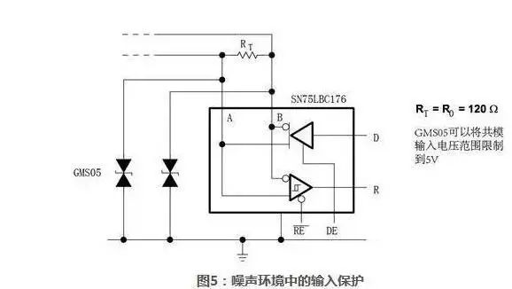
RT is usually the termination resistor equal to the cable characteristic impedance R0.
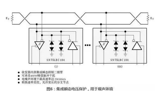
Figure 6 shows the 485 transceiver SN75LBC184 with integrated transient suppression diodes, suitable for situations where full 485 functionality is desired but PCB space is limited. The SN75LBC184 integrates protection diodes for high-energy electrical noise environments and can directly replace the SN75LBC176.
2.3.2 Failure Protection
Many 485 applications also require failure protection, which is very useful at the application layer and needs to be carefully considered and fully understood.
In any interface system where multiple drivers/receivers share the same bus, the drivers are mostly inactive, a state known as the bus idle state. When the driver is in the idle state, the driver output is in a high-impedance state. When the bus is idle, the line voltage is in a floating state (i.e., it is uncertain whether it is high or low). This can cause the receiver to be incorrectly triggered as high or low (depending on the environmental noise and the last level polarity before the line floated). Clearly, this situation is undesirable. There needs to be relevant circuitry in front of the receiver to turn this uncertain state into a known, pre-agreed level, which is called failure protection. Additionally, failure protection must also prevent data errors caused by short circuits.
There are many methods to achieve failure protection, including adding hardware circuits and using software protocols. Although implementing software protocols is more complex, it is the preferred method. However, since most system designers and hardware designers prefer to implement failure protection using hardware, adding hardware circuits for failure protection is more commonly used.
Regardless of whether a short circuit or open circuit occurs, the failure protection circuit must provide a clear input voltage for the receiver. If the communication line is in a very harsh environment, line termination matching is also necessary.
Currently, many manufacturers are beginning to integrate some failure protection circuits (such as open-circuit failure protection) into the chip. Typically, these additional circuits only add a high-value pull-up resistor at the non-inverting input of the receiver and a high-value pull-down resistor at the inverting input of the receiver. These two resistors are usually around 100KΩ, and these resistors and the termination matching resistor form a potential driver that can only provide a few mV of differential voltage. Therefore, this voltage (receiver threshold voltage) is not sufficient to switch the receiver state. Using such internal pull-up and pull-down resistors allows the bus to operate without termination matching but significantly reduces the maximum signal rate and reliability.
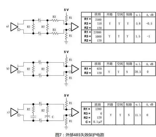
Figure 7 provides some common external failure protection circuits for the 485 interface, each circuit strives to maintain the receiver input voltage above the minimum threshold and maintain a known logic state under one or more fault conditions (open circuit, idle, short circuit). In these circuits, R2 represents the transmission line impedance matching resistor and becomes part of the voltage driver: generating a steady-state bias voltage. Here, it is assumed that each receiver represents one unit load.
The table on the right side of Figure 7 lists some typical resistor and capacitor values, the types of failure protection provided, the number of unit loads used, and signal distortion. In the next section, the resistance values in the short-circuit failure protection circuit will be calculated to illustrate how to modify these resistance values for specific designs.
To achieve short-circuit protection, more resistors are needed. When the cable is short-circuited, the transmission line impedance becomes zero, and the termination matching resistor is also shorted. Adding extra resistors in series at the receiver input can achieve short-circuit failure protection.
Figure 8 shows that the additional resistor R3 can only be used in cases where the driver and receiver are separated. Most 485 drivers and receivers are now integrated into a single chip (called a transceiver) and are internally connected to the same bus, making it impossible to use short-circuit failure protection with such transceivers. If short-circuit protection is needed, a transceiver with integrated short-circuit protection can be chosen, or separate driver and receiver devices, such as SN75ALS180, can be used. If short-circuit failure protection circuits are used in transceivers, resistor R3 will cause additional distortion in the output signal. Separate driver and receiver devices like SN75ALS180 will not have this issue because the driver is directly connected to the bus, bypassing R3.
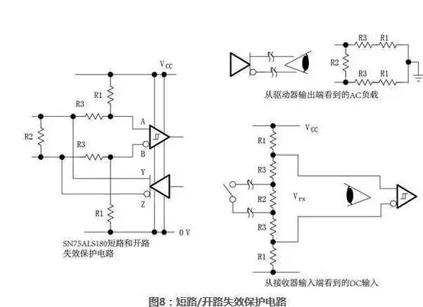
Next, we will calculate the resistance values. If the transmission line is short-circuited, R2 is removed from the circuit, and the input voltage at the receiver is:
VID= VCC * 2R3 / (2R1 + 2R3)
For 485 applications, the standard specifies that the receiver can recognize input signals as low as 200mV. Therefore, when VID > VIT or VID > 200mV, a known state can be determined. This is the first design constraint:
VCC* 2R3 / (2R1 + 2R3) > 200mV
When the transmission line is in a high-impedance state, the receiver is affected by R1, R2, and R3, and its input voltage is:
VID= VCC* (R2 + 2R3) / (2R1 + R2 + 2R3)
This gives the second design constraint:
VCC * (R2 + 2R3) / (2R1 + R2 + 2R3) > 200mV
The transmission line will be affected by the termination matching resistor R2 and twice the (R1+R3) in parallel. The characteristic impedance Zo of the transmission line must match this, leading to the third design constraint:
Zo= 2R2 * (R1 + R3) / (2R1 + R2 +2R3)
Other design constraints include additional line loading provided by the failure protection circuit, signal distortion caused by R3 and R1, and the input resistance of the receiver.
Note: 3.3V 485 transceivers such as SN75HVD10 and newer products have integrated short-circuit/open-circuit failure protection circuits.
2.4 Current Isolation
Computers and industrial serial interfaces are often in noisy environments, which may affect the integrity of data transmission. For any interface circuit, a tested method to improve noise performance is current isolation.
In data communication systems, isolation refers to the absence of direct current flow between multiple drivers and receivers. Isolation transformers provide power to the system, while optocouplers or digital isolator devices provide data isolation. Current isolation can eliminate ground loops and suppress noise voltages. Therefore, using this technique can suppress common-mode noise and reduce other radiated noise.
For example, Figure 9 shows a node in a process control system, connecting a data logger and a main computer via a 485 link.
When a nearby motor starts, the ground potential of the data logger and computer may momentarily differ, which can often cause a large current. If data communication does not adopt an isolation scheme, data may be lost, and in worse cases, the computer may be damaged.
2.4.1 Circuit Description
The schematic shown in Figure 9 is a node in a distributed monitoring, control, and management system, which is commonly used in process control. Data is transmitted via a pair of twisted wires, and the ground wire uses a shielding layer. Such applications often require low power consumption, as many remote stations use batteries or require backup batteries (the device must be able to operate for a certain time using a backup battery after a power outage). Additionally, using low-power counts allows for the use of small isolation transformers. As shown in Figure 9, the transceiver uses SN65HVD10; of course, any TI 3.3V or 5V RS485 transceiver, 3.3-V TIA/EIA-644 LVDS, or 3.3-V TIA/EIA-899 M-LVDS transceiver can be used in this circuit.
2.4.2 Operating Principle
The example shown in Figure 9 can be used for 3.3V or 5V, with the power supply isolated by a transformer, and the data signal isolated by a digital isolator. Since the 485 transceiver requires an isolated power supply, an adjustable LDO voltage regulator must be isolated. This function can be achieved by using a NAND gate oscillator circuit to drive the isolation transformer. The output voltage of the transformer is adjusted and filtered for use by the low-dropout linear regulator. In high EMI environments, this method is commonly used to prevent noise coupling from other long-distance powered electronic systems to the main power supply. TPS7101 is used to power other electronic components, providing up to 500mA of current. By adjusting the bias resistor R7, TPS7101 can output 3.3V or 5V, with specific resistance values listed in the BOM.
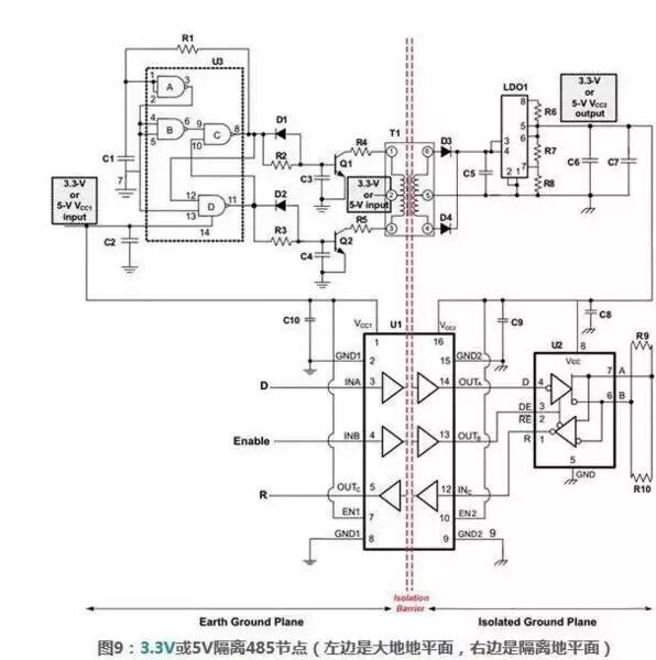
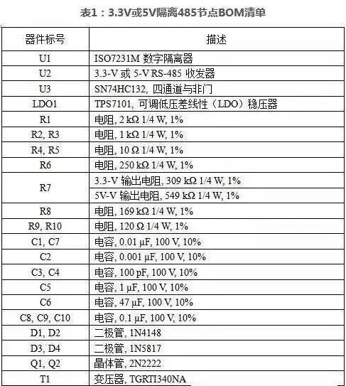
The data signal isolation is completed by the three-channel digital isolator ISO7231M. This device can provide 2.5KV (rms) voltage isolation and 50KV/us transient immunity at a signal rate of 150Mbps.
3.Example of Process Control Design
To gain more knowledge about 485 system design, a good approach is to look at specific examples. Consider a system with a capacity of one master controller and several sub-stations in a factory automation system, where each sub-station can send and receive data.
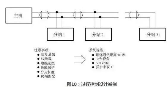
The system characteristics are as follows, with general specifications shown in Figure 10.
-
Farthest sub-station is 500 meters from the master controller
-
31 sub-stations (32 devices in total including the master)
-
Signal transmission rate is 500 kbit/s
-
Half-duplex communication
Devices following the 485 standard transmit data at 500 kbit/s, requiring the driver output transition (rise/fall) time tt not to exceed 0.3 unit interval (UI), so:
tt ≤ 0.3 * UI
tt ≤ 0.3 * (1 /(500 * 103)) = 600ns
If the signal transmission speed in the cable equals the speed of light in a vacuum, the signal transmission delay tpd is 3.33ns/m, multiplied by the transmission line length of 500 meters, resulting in 1667ns.
According to section 2.1, it can be determined whether the transmission line is a distributed parameter model or a lumped parameter model: if 2tpd ≥ tt/5, the transmission line is considered a distributed parameter model. Clearly, 3334 > 120, so the transmission line model in this example is a distributed parameter model. In industrial environments, such transmission lines must have termination matching.
Regarding attenuation, although the fundamental frequency of the signal rate of 500 kbit/s is 250 kHz, we still calculate attenuation at 500 kHz because the signal actually contains higher frequency components. According to the maximum attenuation rule of not exceeding -6dB, the maximum attenuation at the end of the 500-meter cable must be less than -6dB, i.e., 0.36dB/30 meters. We refer to the chart shown in Figure 3, which is provided by the cable manufacturer, showing the relationship between attenuation and frequency. The attenuation corresponding to 500 kHz frequency is more than 0.5dB/30 meters, exceeding the design constraint of 0.14dB/30 meters. In this case, this is acceptable because slightly reducing the noise margin provided by conservative rules is permissible.
This article is reprinted from the internet, copyright belongs to the original author. If you find it unsatisfactory, please contact us for deletion!
↙↙↙Click here