Basic Knowledge of FPC/PCB
Introduction to Circuit Boards
1. Flexible Printed Circuit Boards
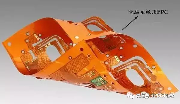
Flexible Printed Circuit Boards (FlexPrintCircuit, abbreviated as “FPC”) are printed circuit boards made of flexible substrates that can be single-sided, double-sided, or multi-layered. They feature characteristics of being lightweight, thin, short, small, high density, high stability, and flexible structure. They can not only bend statically but can also bend dynamically, roll, and fold.
2. Rigid Printed Circuit Boards
Rigid Printed Circuit Boards (PrintedCircuitBoard, abbreviated as “PCB”) are printed circuit boards made from rigid substrate materials that are not easily deformed and remain flat during use. They have advantages of high strength, resistance to warping, and secure mounting of surface-mounted components.
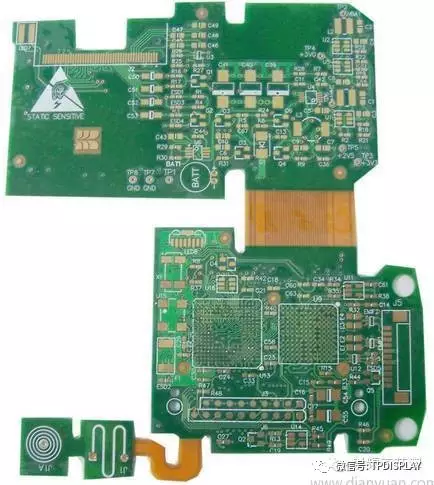
 Rigid-Flex boards (RigidFlex) are special flexible printed circuit boards formed by selectively laminating rigid and flexible substrates together. They have a compact structure with metallized holes forming electrical connections. They feature high density, fine lines, small apertures, compact size, lightweight, and high reliability, maintaining stable performance in environments with vibration, impact, and humidity. They can be bent and installed in three dimensions, effectively utilizing installation space, and are widely used in portable digital products such as mobile phones, digital cameras, and digital camcorders. Rigid-Flex boards are increasingly used in packaging reduction, especially in consumer areas.
2. Introduction to Circuit Board Materials
1. Conductive Medium:Copper (CU)
﹣Copper Foil:Rolled Copper (RA), Electrolytic Copper (ED), High Ductility Electrolytic Copper (HTE)
﹣Thickness:1/4OZ, 1/3OZ, 1/2OZ, 1OZ, 2OZ, these are common thicknesses
﹣OZ (Ounce):Unit of copper foil thickness; 1OZ = 1.4 mil
2. Insulation Layer:Polyimide (PI), Polyester, Polyethylene Naphthalate (PEN)
﹣The most commonly used is Polyimide (abbreviated as “PI”)
﹣PI Thickness:1/2mil, 1mil, 2mil, these are common thicknesses
﹣1 mil = 0.0254mm = 25.4um = 1/1000 inch
3. Adhesive:Epoxy resin, Acrylic resin.
﹣The most commonly used is epoxy resin, thickness varies depending on different manufacturers.
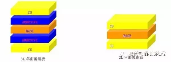
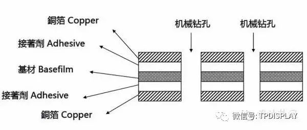
4. Copper Clad Laminate (Cuclad laminates, abbreviated as “CCL”):
﹣Single-sided copper clad laminate: 3LCCL (with adhesive), 2LCCL (without adhesive), as illustrated below.
﹣Double-sided copper clad laminate: 3LCCL (with adhesive), 2LCCL (without adhesive), as illustrated below.
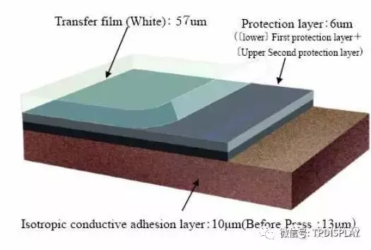
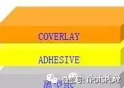
5. Cover Film (Coverlay, abbreviated as “CVL”):Composed of insulation layer and adhesive, covering the conductive lines to provide protection and insulation. The specific lamination structure is as follows:
2. Conductive Silver Foil:Electromagnetic Wave Protection Film
﹣Type:SF-PC6000 (black, 16um)
﹣Advantages:Ultra-thin, good sliding and bending performance, suitable for high-temperature reflow soldering, and good dimensional stability.
The commonly used is SF-PC6000, the lamination structure is as follows:
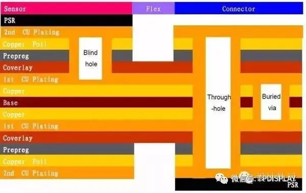
3. Rigid-Flex Lamination Display
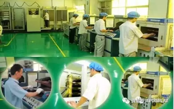
4. Circuit Board Manufacturing Process
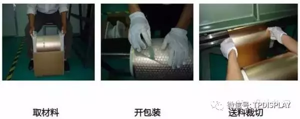
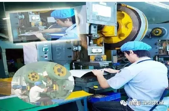
1) Cutting: Shearing Cutting/SHEARING
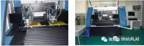
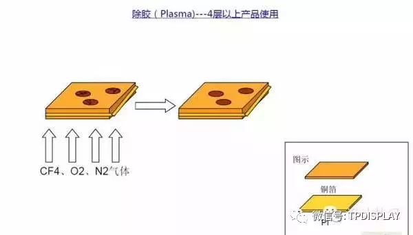
2) CNC DrillingCNC DRILLING
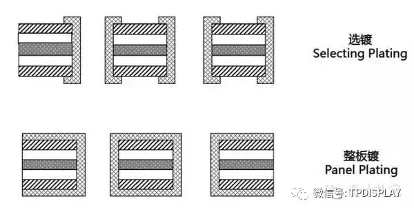
3) Plating Through HolePLATING THROUGH HOLE
4) DES Process(Five Steps)
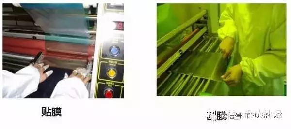
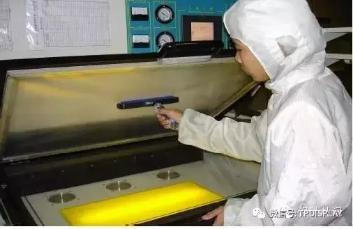
(1). Film Application(Dry Film Application)
Working Environment:Yellow Light
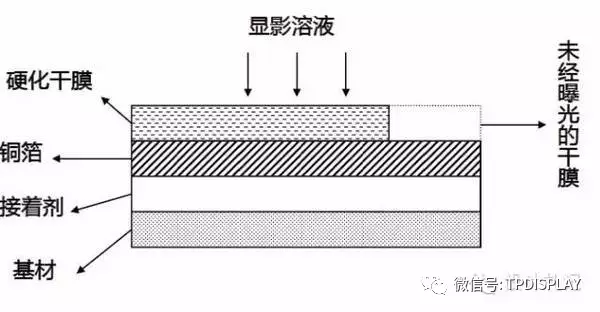
Purpose:Through UV light exposure and film blocking, the areas where the film is transparent undergo optical polymerization reactions, while the areas where the film is brown cannot undergo optical polymerization reactions due to UV light not penetrating.
Working Solution:Na2CO3 (K2CO3) weak alkaline solution
Purpose:To wash away the undeveloped dry film parts using a weak alkaline solution
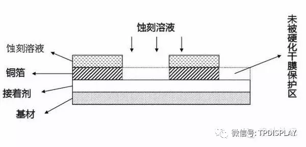
Working Solution:Acidic Hydrogen Peroxide: HCl + H2O2
Purpose:To etch away the copper exposed after development using the chemical solution, forming the pattern transfer.
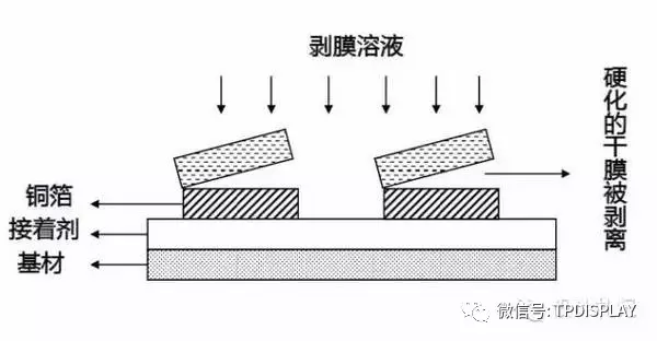
Working Solution:NaOH strong alkaline solution
Main Equipment:AOI, VRS System
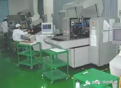
Formed circuit copper foil must undergo AOI system scanning to detect circuit deficiencies. Standard circuit image data is stored in the AOI mainframe, and the CCD optical camera scans the circuit information on the copper foil and compares it with the stored standard data. If anomalies are found, the locations of the anomalies are numbered and recorded for transmission to the VRS mainframe. The VRS will magnify the copper foil 300 times, displaying the recorded defect locations sequentially for the operator to determine if they are genuine defects. Genuine defects will be marked with a water-based pen for subsequent personnel to categorize, count, and repair. Operators use a 150x magnifying glass to classify defect types, compile statistics, and generate quality reports, providing feedback to the previous process for timely improvement measures. Due to fewer defects in single-sided boards and lower costs, it is difficult to use AOI for interpretation, so manual visual inspection is used.
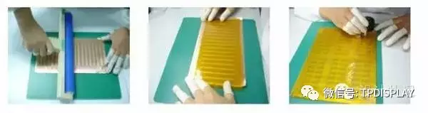
 Protective Film Function:
1) Insulation, anti-solder effect;
2) Protect circuit lines;
3) Increase flexibility of soft boards, etc.
Working Conditions:High temperature and high pressure
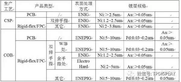
After hot pressing, surface treatment must be performed on the exposed copper foil areas.
The method is determined according to customer requirements
10) Testing (O/S Detection)
Testing fixtures + testing software perform a full functional inspection of the circuit board
Corresponding Shape Film Tools:Knife film, laser cutting, etching film, simple steel mold, steel mold
Processing assembly refers to assembling materials according to customer requirements, such as:
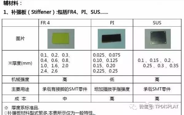
A. Stainless Steel Reinforcement
B. Beryllium Copper Sheets/Phosphor Copper Sheets/Nickel-Plated Steel Sheets Reinforcement
Inspection Items:Appearance, dimensions, reliability
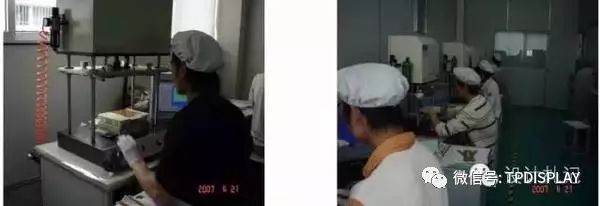
Testing Tools:Two-dimensional, micrometer, caliper, magnifying glass, soldering furnace, tensile tester
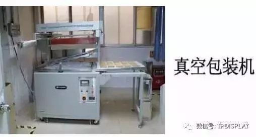
1. Plastic bag + cardboard
2. Low-adhesive packaging materials
4. Special vacuum box (anti-static grade)
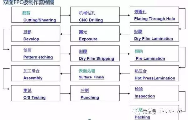
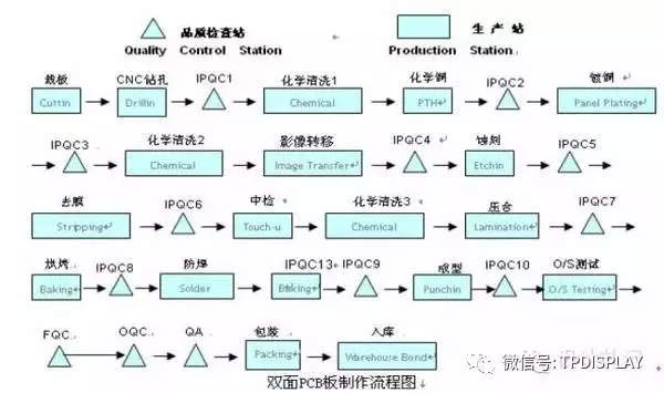
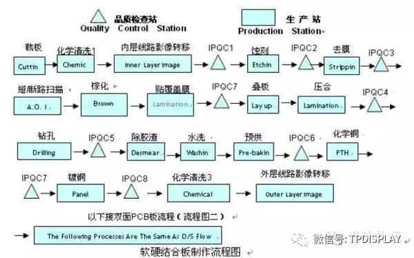
Flowchart of Double-Sided PCB Manufacturing
Flowchart of Rigid-Flex Board Manufacturing
The copyright of this article belongs to the original author and does not represent the association’s viewpoint. The articles promoted by the “Jiangxi Province Electronic Circuit Industry Association” are for sharing purposes only and do not represent the stance of this account. If there are copyright issues, please contact us for deletion.
Protective Film Function:
1) Insulation, anti-solder effect;
2) Protect circuit lines;
3) Increase flexibility of soft boards, etc.
Working Conditions:High temperature and high pressure
After hot pressing, surface treatment must be performed on the exposed copper foil areas.
The method is determined according to customer requirements
10) Testing (O/S Detection)
Testing fixtures + testing software perform a full functional inspection of the circuit board
Corresponding Shape Film Tools:Knife film, laser cutting, etching film, simple steel mold, steel mold
Processing assembly refers to assembling materials according to customer requirements, such as:
A. Stainless Steel Reinforcement
B. Beryllium Copper Sheets/Phosphor Copper Sheets/Nickel-Plated Steel Sheets Reinforcement
Inspection Items:Appearance, dimensions, reliability
Testing Tools:Two-dimensional, micrometer, caliper, magnifying glass, soldering furnace, tensile tester
1. Plastic bag + cardboard
2. Low-adhesive packaging materials
4. Special vacuum box (anti-static grade)
Flowchart of Double-Sided PCB Manufacturing
Flowchart of Rigid-Flex Board Manufacturing
The copyright of this article belongs to the original author and does not represent the association’s viewpoint. The articles promoted by the “Jiangxi Province Electronic Circuit Industry Association” are for sharing purposes only and do not represent the stance of this account. If there are copyright issues, please contact us for deletion.