The Audi A8, as the world’s first mass-produced car equipped with Level 3 autonomous driving, still holds significant relevance today. The latest teardown of the zFAS reveals that achieving higher levels of autonomous driving is more challenging from both technical and economic perspectives than anyone initially expected. The entire automotive industry is still facing the technical issues and unfamiliar cost structures that Audi encountered.From the teardown and reverse cost calculation by SystemPlus, the semiconductor costs in the zFAS account for 60%, approximately $290. However, what is truly shocking, and for which no automotive company is prepared, is that they must allocate 50% of the component profits to pay for flagship chip solutions provided by companies like Nvidia and Intel.In the past 18 months, some leading OEM manufacturers have begun to hint that they wish to design their own autonomous driving chips (like Tesla). This approach allows them to control their destiny in hardware and software development. However, given the high costs of chip design, it remains unclear whether OEM manufacturers can better address this issue.When the Audi A8 was launched, its in-car technology was referred to as a “breakthrough in autonomous driving,” featuring a system called Traffic Jam Pilot. Once activated, Traffic Jam Pilot can alleviate the driver’s troubles in congested traffic. However, this idea conflicts with the “handover issue” (after ending the congestion autonomous driving mode, Audi stated that the handover time is 10 seconds. The system will issue visual and auditory prompts requiring the driver to take over). The handover issue has always plagued Level 3 vehicles.Today, there is not a single A8 on the streets with the Level 3 driving function activated and operational.However, this is not a blow to Audi; the A8 highlights the challenges faced by autonomous driving, and industry leaders must figure out the complexities related to various regulations, technology, safety, behavior, legal, and business aspects before they can boast about the future of driverless cars. This partly explains the momentum behind OEMs, Tier One suppliers, chip vendors, and technology service companies establishing safety standards.Under the Hood of the A8Challenges faced by automotive manufacturers will no longer be about providing the fastest 0 to 100 km/h speed or the best acceleration, but rather ensuring increasingly advanced autonomous driving and assistance systems. This is the goal of the Audi A8, which features Level 3 autonomous driving capabilities and is the first vehicle to use lidar technology.The A8’s sensor suite also includes cameras, radar, and ultrasonic sensors (as shown in Figure 1). In congested traffic, the Audi A8 can achieve autonomous driving without driver intervention. Audi stipulates that the driver does not need to keep their hands on the steering wheel and, according to local regulations, can engage in other activities, such as watching TV in the car. The vehicle can perform most driving tasks but still requires human operation.
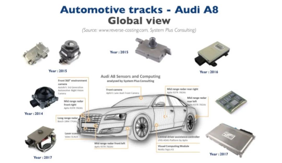
Figure 1 Key Elements of the Audi A8Fraux wrote in the Audi A8’s innovation technology ranking: “Audi is the first car with Level 3 autonomy. The Traffic Jam Pilot system installed in the Audi A8 is responsible for using sensor fusion technology and the world’s first laser scanner to drive at low speeds on highways and expressways at 60 km/h. (Note: As of now, this Level 3 function has not been activated).L3 Autonomous Driving Computing PlatformThe Audi A8’s autonomous driving system consists of a series of sensors and a zFAS controller provided by Ambarella. The zFAS (as shown in Figure 2) is a centralized computing platform that serves as a central hub for processing ultrasonic sensors (front, rear, and side), 360-degree surround cameras, mid-range radar, long-range radar, and a laser scanner located at the front of the vehicle.
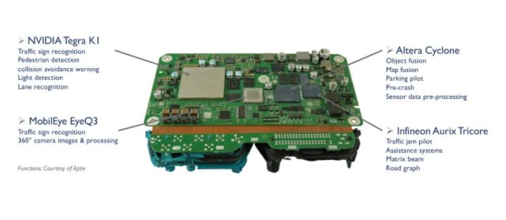
Figure 2 Audi A8 in the FAS ControllerProcessing Chips in the zFAS ControllerThe platform processor in the zFAS controller is the Nvidia Tegra K1 (as shown in Figure 3), used for traffic signal recognition, pedestrian detection, collision warning, traffic light detection, and lane recognition. The Tegra K1, with an eight-layer PCB, integrates 192 CUDA cores, the same number as the single SMX module integrated into Nvidia’s Kepler GPU currently on the market, supporting DirectX 11 and OpenGL 4.4.
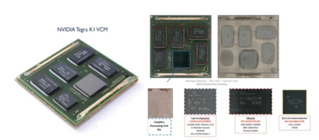
Figure 3 Nvidia Tegra K1The Intel/Mobileye EyeQ3 is responsible for image processing. To meet power consumption and performance goals, the EyeQ SoC is designed using finer geometries. In the EyeQ3, Mobileye uses 40 nm CMOS, while the company will use 7nm FinFET in the fifth generation SoC EyeQ5. Each EyeQ chip has heterogeneous, fully programmable accelerators, with each type of accelerator optimized for its own series of algorithms.In addition to the Nvidia Tegra K1 and Mobileye EyeQ3, the zFAS also employs Altera Cyclone for data preprocessing and Infineon Aurix Tricore for monitoring safety operations. The Altera Cyclone series FPGA devices are based on a 1.5V, 0.13µm full-layer copper SRAM process, with densities of up to 20,060 logic elements (LE) and 288kbit RAM.The Infineon Aurix architecture achieves performance optimization in powertrain and safety applications in the automotive industry. TriCore is the first unified single-core 32-bit microcontroller-DSP architecture optimized for real-time embedded systems.Sensors of the A8For the automotive industry, advanced driver assistance systems have become a necessity for all new cars to achieve higher European NCAP ratings. In Figure 1, we can find a detailed list of the equipment in the Audi A8. Sensor manufacturers are developing increasingly efficient radar sensors, with companies like Aptiv, Veoneer, ZF, Valeo, Bosch, Mando, Denso, and Ainstein currently offering radar sensors on the market.On the Audi A8, we can see Autoliv’s third-generation automotive night vision camera, Aptiv’s lane assist front camera, Valeo’s Scala laser scanner, Bosch’s LRR4 77GHz long-range radar sensor, and Aptiv’s R3TR 76 GHz mid-range radar.The Autoliv night vision camera consists of a camera and a remote processing unit (as shown in Figure 4), where the infrared night vision camera is composed of FLIR’s 17um pixel high-definition vanadium oxide microbolometer ISC0901, which is based on a complex optical system and FPGA array with custom algorithms for complex numerical processing.
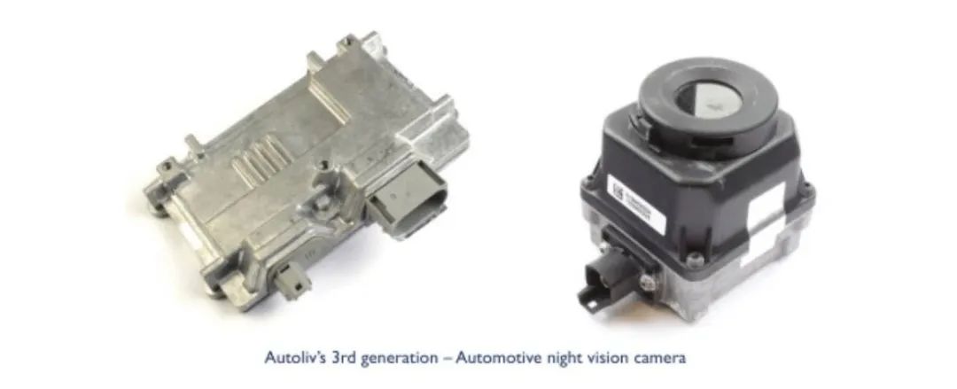
Figure 4 Autoliv’s Third-Generation Automotive Night Vision CameraAptiv’s lane assist front camera (as shown in Figure 5) is mounted on the rearview mirror, with an effective range of 80 meters and a capture speed of 36 images per second. This camera uses a 1.2M pixel CMOS image sensor provided by ON Semiconductor and an 8-bit Microchip PIC microcontroller. The zFAS control unit uses the Mobileye EyeQ3 processing chip to manage image and recognition software.
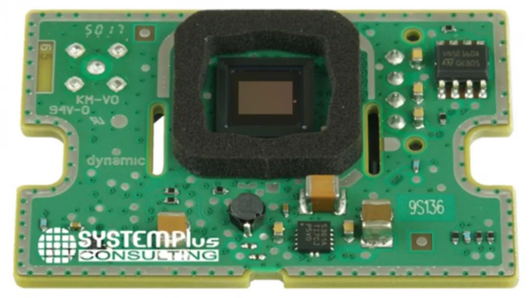
Figure 5 PCB of Aptiv’s Lane Assist Front CameraLRR4 is a multi-mode radar with six fixed radar antennas from Bosch (as shown in Figure 6). Four centrally arranged antennas provide high-speed recording of the environment, creating focused beams with an aperture angle of ±6 degrees, minimizing traffic interference in adjacent lanes. In the near field, the two external antennas of the LRR4 expand the field of view to ±20 degrees, providing a range of 5 meters, capable of quickly detecting vehicles entering or leaving the lane.

Figure 6 Long-Range Radar SensorAptiv’s short-range radar sensor consists of two transmitter channels and four receiver channels, operating in the 76-77 GHz band, which is the standard configuration for automotive radar applications. The PCB uses monolithic microwave integrated circuits (MMIC) and cavity waveguides, and the RF printed circuit board (PCB) substrate uses glass-reinforced hydrocarbon ceramic laminates, completely free of PTFE (as shown in Figure 7).
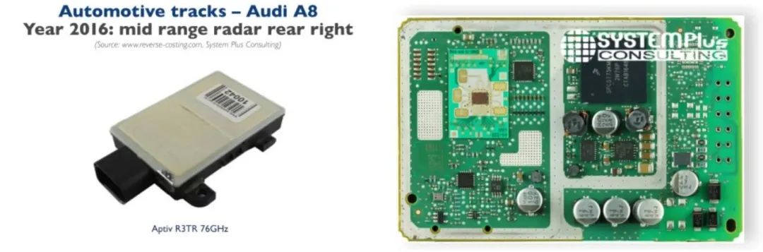
Figure 7 Aptiv R3TRA key element of the Audi A8 is the lidar. This is the first time an automotive manufacturer has used a laser scanner. It is based on a mechanical system with rotating mirror technology and edge-emitting technology at a wavelength of 905 nm. The device has a range of 150 meters, a horizontal field of view angle of 145°, and a vertical field of view angle of 3.2°. The motor control unit consists of a stator and rotor with a control driver and an MPS40S Hall sensor for motion detection. The Hall effect sensor responds to magnetic fields by changing its output voltage. This is a durable solution as there are no mechanical parts that wear out over time. The integrated software package reduces the size of the system and the relative complexity of implementation (as shown in Figure 8).
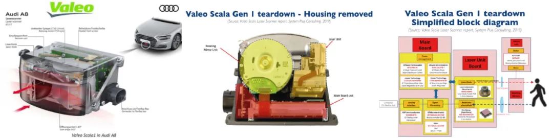
Figure 8 Laser Scanning DeviceThe lidar system measures the time of flight of the transmitted laser to accurately measure timing (as shown in Figure 9). Recent developments have seen several multi-beam lidar systems that can generate precise three-dimensional images of the environment around the vehicle.
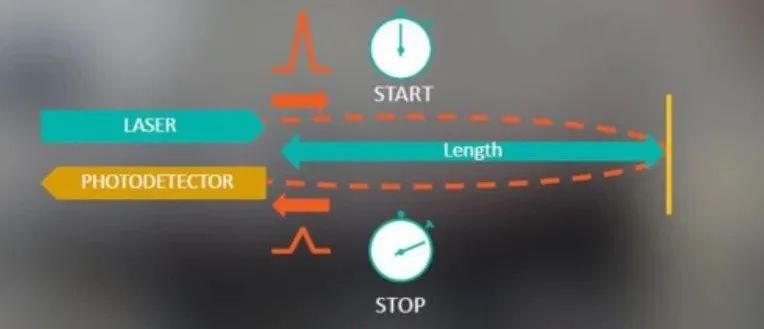
Figure 9 Ranging PrincipleEdge-emitting lasers are the original and still widely used form of semiconductor lasers. Their resonant lengths can achieve high gain. Within this structure, the laser beam is guided in a typical double heterostructure waveguide structure. Depending on the physical characteristics of the waveguide, it is possible to achieve high beam quality but limited output power, or high output power but low beam quality (as shown in Figure 10).
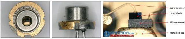
Figure 10 Edge-Emitting Laser DiodeThe lasers used in lidar solutions have a 3-pin TO package, with a chip area of 0.27 mm², as shown. The laser’s power is 75 W, with a diameter of 5.6 mm. It is likely that Sheaumann manufactures the laser components for 100 mm wafers. The adjustment unit uses an avalanche photodiode (APD) to capture the laser beam after passing through two lenses (one for emission and one for reception). The APD may be made by First Sensor on a 150 mm wafer with an 8-pin FR4 LLC package and a chip area of 5.2 mm² (as shown in Figure 11).The APD is a high-speed photodiode that uses photon multiplication to obtain low-noise signals. The APD has a higher signal-to-noise ratio than a PIN photodiode and can be used in various applications, such as high-precision rangefinders and low-light detection. From an electronic perspective, the APD requires a higher reverse voltage and requires more detailed consideration of its temperature-dependent gain characteristics.
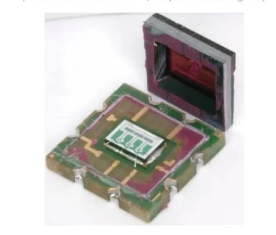
Figure 11 Avalanche Photodiode (APD)In addition to the two units used for laser and motion control, the control hardware also includes a motherboard, which includes a Xilinx XA7Z010 SoC dual-core ARM Cortex-A9, a 32-bit STMicroelectronics SPC56EL60L3 microcontroller, and a power management system, which includes ADI’s synchronous buck regulator, Infineon’s dual-channel smart high-side power switch, ADI’s three-way buck IC with LDO, and Allegro’s three-phase sensorless fan driver IC. The FlexRay protocol supports data communication. The FlexRay system consists of several electronic control units, each with a controller to manage access to one or two communication channels.It is estimated that this lidar technology, if produced in quantities of 100,000, could cost around $150, a significant portion of which is related to the motherboard and laser (as shown in Figure 12).
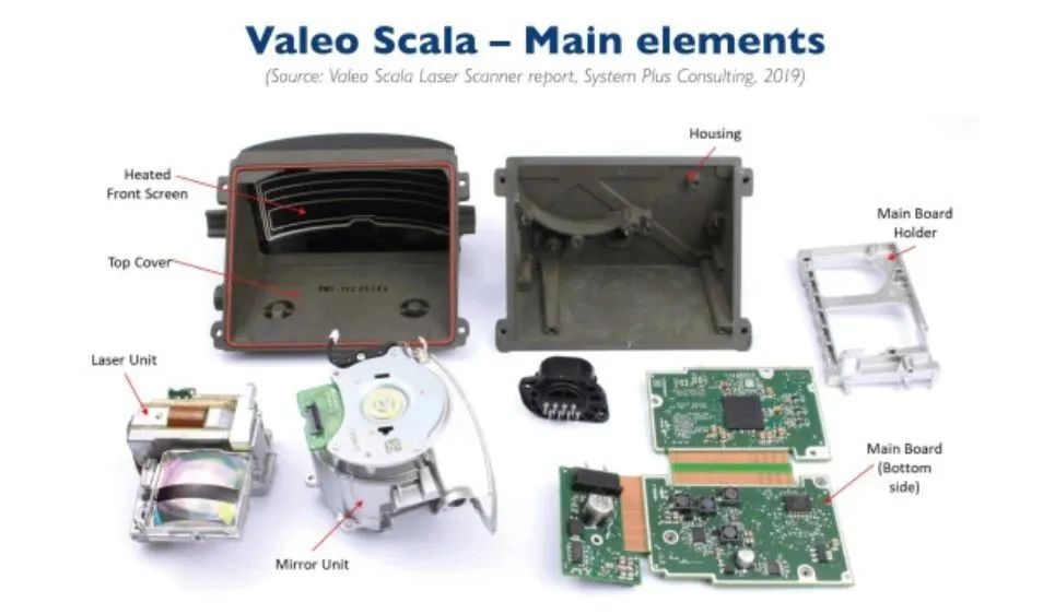
Figure 12 Disassembled Laser Scanner HardwareIn lidar projects, transimpedance amplifiers are the most critical part of the electronic layout. Low noise, high gain, and fast recovery characteristics make these new devices ideal for automotive applications. To achieve optimal performance, designers must pay special attention to interface and integrated circuit, wavelength, and optical-mechanical alignment issues. These integrated circuits comply with AEC-Q100 certification to meet the strictest safety requirements in the automotive industry.Recommended Reading
We have all been asleep, and next we will bleed
BMW: Autonomous Driving Controller Hardware Architecture
Volkswagen: Electronic and Electrical Architecture of the MEB Platform
Audi A8’s zFAS Controller (Video)
 —END—
—END—

If you found this helpful, please click the lower right cornerto read.