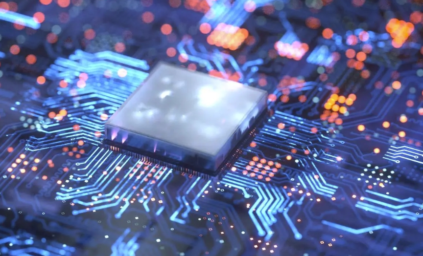
In semiconductor processes, 3D printing technology, with its advantages of high precision and high freedom in manufacturing, has penetrated multiple key areas, driving the industry towards miniaturization, integration, and efficiency. The following are its main application fields and specific practices:
1. Prototyping and Rapid Validation
Application Scenario: Traditional semiconductor prototyping relies on complex processes such as photolithography and etching, which are time-consuming and costly. 3D printing can quickly produce high-precision prototypes, accelerating design iterations.
Case Study: A team from Tsinghua University achieved 3D nano-printing of semiconductor quantum dots using photochemical bonding technology, with a resolution of 150 nanometers, allowing for direct validation of three-dimensional optoelectronic chip designs, thus shortening the R&D cycle.
2. Manufacturing of Complex Structures
Micro-Electro-Mechanical Systems (MEMS): 3D printing can manufacture tiny interconnection structures, sensors, and actuator integration structures that are difficult to achieve with traditional processes. For example, the micro-nano probe array printed by Exaddon AG in Switzerland has a spacing of less than 20 micrometers, significantly improving testing efficiency.
Three-Dimensional Integrated Chips: By printing layer by layer, vertical stacking of transistors and interconnection layers is achieved, breaking through the limitations of two-dimensional planar integration.
3. Packaging and Testing Stages
Advanced Packaging Technology: 3D printing supports 2.5D/3D stacked packaging, optimizing thermal management and signal transmission. For instance, Exaddon AG’s μAM technology directly prints high-conductivity structures on micro PCBs, shortening connection distances and reducing latency.
Testing Structures: High-precision test probes and fixtures are printed, such as a MicroLED test array with a spacing of 18.5 micrometers, enhancing testing accuracy and efficiency.
4. Optimization of Manufacturing Equipment and Tools
Thermal Management Components: 3D printing enables the creation of wafer tables and heat exchangers with conformal cooling channels, improving equipment precision and stability. 3D Systems has achieved an 83% reduction in thermal variation of wafer tables through topological optimization design, with precision reaching 1-2 nanometers.
Lightweight Components: The ASML lithography machine chuck has been reduced in weight by 30% through 3D printing, increasing positioning speed and production capacity.
5. Development of New Materials and Devices
Ceramic Material Applications: 3D printing of ceramic components such as silicon nitride and alumina is used for high-temperature, high-power semiconductor packaging. For example, ceramic thermal management components printed by Qiyu Technology exhibit excellent thermal conductivity, suitable for extreme environments.
Heterogeneous Material Integration: 3D printing technology enables the mixed printing of semiconductors with metals and polymers, expanding device functionality.
6. Small-Batch Customized Production
Application Scenario: For research or small-batch high-end chip demands, 3D printing reduces mold costs and enables rapid customization. For instance, printing photonic crystal sensors with specific wavelengths to meet personalized requirements.
Technical Challenges and Future Trends
Precision and Materials: There is a need to break through nano-level printing precision and to be compatible with more semiconductor materials (such as silicon and compound semiconductors).
Industrialization Path: It is necessary to optimize printing speed, reduce costs, and integrate with existing processes (such as photolithography).
Industry Layout: Giants like Nikon and ASML have accelerated technology integration by acquiring 3D printing companies (such as SLM Solutions), promoting innovation in semiconductor manufacturing.
Conclusion: 3D printing technology is reshaping semiconductor processes, from prototype design to mass production packaging, with advantages in complex structure manufacturing, thermal management optimization, and material innovation. As the technology matures, it is expected to play a greater role in fields such as three-dimensional integrated chips and quantum devices in the future.
************(End)************May everyone we meet, every experience we have, and everything we see become better because of our existence.May our great motherland always prosper!May our lovely life continue to be beautiful!