 Printed Circuit Board (PCB) design is a crucial aspect of modern electronic products and serves as the foundation for the development and manufacturing of electronic devices. PCBs are the backbone of electronic products, providing necessary interconnections and support for various components. The PCB design process includes creating layouts to optimize component placement, routing of traces, and ensuring the overall functionality and reliability of the circuit.
This series delves into the complexities of PCB design, covering a wide range of topics that are essential for both beginners and experienced designers. Details are as follows:
- The first part establishes a solid foundation, exploring the design workflow—from schematic capture to layout and key design rule checks.We will examine PCB components and layers, followed by signal integrity and thermal management—critical for creating high-performance PCBs.
- The second part will focus on turning PCB designs into reality, exploring the complexities of PCB manufacturing, assembly, testing, and debugging.Finally, we will lay the groundwork for creating high-performance electronic devices using industry-leading PCB design software and tools.
Let’s start with the basics of PCB design!
PCB design involves creating layouts that define the electrical connections and mechanical structure of electronic devices. Understanding the fundamental concepts and terminology associated with PCB design is crucial for creating reliable and efficient electronic products.
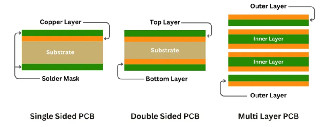 Single-sided, double-sided, and multi-layer PCBsPCBs are classified into different types based on their structure and the number of conductive layers. Single-sided PCBs have components and traces on only one side of the board, while double-sided PCBs utilize both sides for component placement and routing. Multi-layer PCBs consist of three or more conductive layers, allowing for more complex designs and higher component density.The choice of materials used in PCB manufacturing plays a crucial role in the performance and reliability of the final product. The most common substrate for PCBs is FR-4, a glass-reinforced epoxy laminate. Other materials, such as polyimide or high-frequency laminates, can be used for specific applications requiring enhanced thermal stability or improved electrical performance.Layers of a PCB and Their FunctionsA typical PCB consists of multiple layers, each serving a specific purpose in the overall design. Conductive layers are usually made of copper and are used to route electrical signals and power between components. The number and arrangement of these layers depend on the complexity of the design and the required functionality.
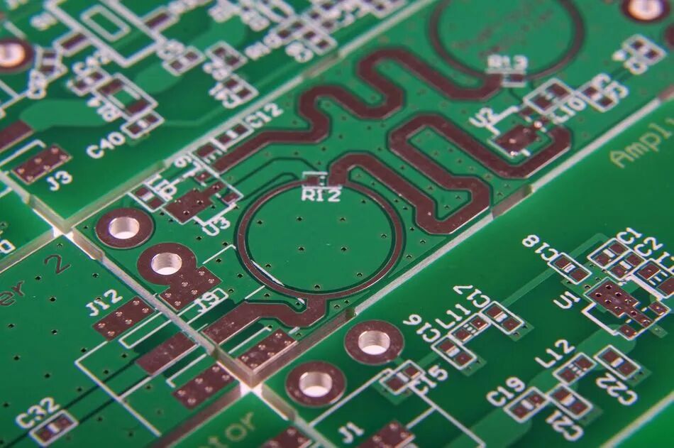 Conductive paths on a printed circuit board (PCB)The layer stack-up design is critical for maintaining signal integrity and ensuring the proper functioning of the PCB. A well-designed layer stack-up considers factors such as signal return paths, impedance control, and crosstalk reduction. Common layer configurations include power and ground layers, signal layers, and dedicated layers for shielding or thermal dissipation.For example, a four-layer PCB may consist of a top signal layer, ground layer, power layer, and bottom signal layer. This configuration provides a stable foundation for signal transmission, reduces electromagnetic interference (EMI) disruption, and facilitates effective power distribution. In more complex designs, additional layers can be added to accommodate higher component densities, high-speed signals, or advanced features such as embedded components or blind/buried vias.PCB Components and Their LayoutPCB design involves the use of various types of components, each serving a specific function in the electronic circuit. These components can be broadly categorized into two main types: through-hole components and surface-mount components. Through-hole components have leads that are inserted into drilled holes on the PCB and soldered on the opposite side, while surface-mount components are placed directly on the surface of the circuit board and soldered.Proper component placement is crucial for achieving optimal performance and reliability in PCB design. When placing components, designers must consider factors such as signal integrity, power distribution, thermal management, and manufacturability. Components should be placed logically, minimizing the distance between related components to reduce signal propagation delays and improve overall circuit performance.Thermal management is another important aspect of component placement. The placement of heat-generating components, such as power regulators or high-speed processors, should allow for effective heat dissipation. This may involve using thermal vias, heat sinks, or other cooling techniques to prevent overheating and ensure reliable operation of the circuit. The Joint Electron Device Engineering Council (JEDEC) has published various thermal management standards for electronic components. Adhering to these standards ensures proper thermal performance and component longevity during the mounting process.Signal integrity is also a key consideration in component layout. The placement of sensitive analog components, high-speed digital components, and power circuits should minimize crosstalk, noise, and electromagnetic interference (EMI). Proper placement of decoupling capacitors near power pins, using ground planes, and separating the analog and digital sections of the PCB can help maintain signal integrity and prevent unnecessary interactions between components.Designers can create PCB layouts that enhance performance, reliability, and manufacturability by considering component layout principles. These layouts can also meet specific application requirements such as signal integrity and thermal management.PCB Design WorkflowThe PCB design workflow is a systematic approach to creating functional and reliable printed circuit boards, from the initial concept to the final manufacturing stage. This workflow involves several key steps, each playing a crucial role in ensuring the success of the project.The first step in the PCB design workflow is the concept design phase, during which the overall requirements and specifications of the electronic product are defined. This phase involves close collaboration between the electrical engineering team, mechanical engineering team, and other stakeholders to establish the functionality, dimensions, and performance characteristics required for the PCB.
Once the concept design is complete, the next step is schematic design, where electrical connections and components are defined using schematic capture tools. This schematic serves as a blueprint for the PCB layout and provides a clear representation of the electrical functionality of the circuit.
After the schematic is completed, the PCB layout process begins. This step involves placing components and routing traces on the circuit board to create a physical representation of the circuit. The layout process must consider various design rules, such as minimum trace width, spacing, and via sizes, to ensure manufacturability and reliability.
Throughout the PCB design workflow, collaboration between different teams is essential. The electrical engineering team works closely with the mechanical engineering team to ensure that the PCB fits within the required enclosure and meets any thermal or structural requirements. The manufacturing team provides input on design for manufacturability (DFM) guidelines to minimize production issues and improve yield.
Once the PCB layout is complete, the design will undergo a series of verification and validation steps, including design rule checks (DRC), electrical rule checks (ERC), and signal integrity simulations. These steps help identify and resolve any potential issues before the design is delivered for manufacturing.
The final step in the PCB design workflow is generating manufacturing files, such as Gerber files and drill files, which the PCB manufacturer uses to produce the physical boards. The manufactured PCBs are tested and assembled before being integrated into the final electronic product.
By following a well-defined PCB design workflow and facilitating collaboration between different teams, designers can create high-quality, reliable, and manufacturable PCBs that meet the specific requirements of the application.
Scheme Design
Schematic design is a critical step in the PCB design workflow as it lays the foundation for the entire project. The purpose of schematic design is to create a graphical representation of the electrical connections and components in the circuit using standardized symbols and notations.
A well-designed schematic should be clear, accurate, and easy to understand, even for those unfamiliar with the specific project. Best practices for creating effective schematics include using consistent naming conventions for components and nets, organizing the schematic into logical hierarchies or functional blocks, and providing clear and concise annotations and comments.
When creating a schematic, designers use various standard symbols to represent different types of components. For example, resistors are typically represented by zigzag lines, while capacitors are shown as two parallel lines. Transistors, diodes, and integrated circuits each have their unique symbols that indicate their specific functions and pin configurations.
In addition to component symbols, schematics also use various types of connectors and labels to indicate how different parts of the circuit are interconnected. For example, power and ground symbols are used to show connections to power and ground planes, while port symbols indicate connections to external devices.
By following best practices and consistent symbols and notations, designers can create schematics that effectively communicate the electrical functionality of the circuit and lay a reliable foundation for the subsequent stages of the PCB design workflow.
PCB Layout
PCB layout is the process of arranging components and routing traces on a printed circuit board to create a functional and manufacturable design. This step is crucial for ensuring the proper operation of electronic products and minimizing potential issues during manufacturing and assembly.
The principles of PCB layout design involve several key considerations, including component placement, trace routing, and via layout. Components should be placed in a logical and organized manner, taking into account factors such as signal integrity, thermal management, and manufacturability.
Proper trace routing is essential for maintaining signal integrity and ensuring reliable operation of the circuit. The way traces are routed should minimize crosstalk, noise, and electromagnetic interference (EMI). High-speed and analog circuits require special attention as they are particularly sensitive to signal degradation and interference.
Via layout is another important aspect of PCB layout design. Vias are small holes drilled in the PCB that provide electrical connections between different layers. Proper via layout helps minimize signal degradation and improve overall circuit performance.
In addition to these general principles, designers must also consider the specific requirements of the application. For example, high-speed digital circuits may require controlled impedance traces and specialized routing techniques to maintain signal integrity. On the other hand, analog circuits may require careful consideration of grounding and shielding to minimize noise and interference.
By following best practices and considering the unique requirements of the application, designers can create PCB layouts that optimize performance, reliability, and manufacturability while meeting the specific needs of electronic products.
Design Rule Check (DRC) and Design for Manufacturability (DFM)
DRC and DFM are two critical aspects of the PCB design workflow that help ensure the integrity and manufacturability of printed circuit boards.
Design Rule Check (DRC)is the process of verifying the PCB layout against a set of predefined design rules (such as minimum trace width, spacing, and via sizes). These rules are established by the PCB manufacturer to ensure that the design can be manufactured without issues. DRC checks help identify potential manufacturing problems, such as short circuits, open circuits, and spacing violations, before the design is sent for manufacturing.
Design for Manufacturability (DFM)is a set of guidelines and best practices that help optimize PCB layouts for efficient and cost-effective manufacturing. DFM considerations include component placement, trace routing, via layout, and the use of specialized features such as blind and buried vias. By following DFM guidelines, designers can minimize manufacturing issues, improve yield, and reduce costs associated with rework and scrap.
Common DRC and DFM rules include:
- Minimum trace width: Traces must be wide enough to carry the required current without overheating or causing voltage drop.
- Minimum spacing: Traces and components must be spaced far enough apart to prevent short circuits and ensure proper solderability.
- Via size: Vias must be large enough to accommodate the required current and provide reliable electrical connections between layers.
- Solder mask clearance: The solder mask must be clear of component pads and traces to ensure proper solderability.
- Annular ring size: The copper around the annular ring or via must be large enough to provide reliable electrical connections and withstand the manufacturing process.
- Component placement: The placement of components should allow for efficient assembly and minimize the risk of manufacturing defects.
- Trace routing: The routing of traces should minimize crosstalk, noise, and electromagnetic interference (EMI).
By following DRC and DFM guidelines, designers can create PCB layouts that are both practical and manufacturable, reducing the risk of manufacturing issues and ensuring a high-quality final product.
Signal Integrity and EMC Considerations
Signal integrity and electromagnetic compatibility (EMC) are two critical aspects of PCB design that directly impact the performance and reliability of electronic products. Signal integrity refers to the ability of signals to propagate through the PCB without distortion or degradation, while EMC involves the ability of electronic devices to operate without causing electromagnetic interference (EMI) or being affected by EMI.
Poor signal integrity and EMC can lead to various issues, including signal distortion, crosstalk, noise, and EMI. These problems can result in device malfunctions, performance degradation, or even complete failure. In some cases, poor EMC can also lead to regulatory compliance issues, as electronic products must meet specific EMC standards to be sold in certain markets.
Several key factors in PCB design affect signal integrity and EMC, including:
- Trace routing: Proper trace routing is essential for maintaining signal integrity and minimizing crosstalk and EMI. High-speed signals should be kept away from sensitive analog circuits and should use appropriate spacing and shielding to minimize interference.
- Grounding and power distribution: A well-designed grounding and power distribution system is crucial for maintaining signal integrity and minimizing EMI. Proper use of ground planes, power planes, and decoupling capacitors helps reduce noise and ensure stable power delivery to components.
- Component placement: Proper component placement helps minimize signal propagation delays, reduce crosstalk, and improve overall signal integrity. Components should be placed close to their related circuits, and sensitive analog components should be separated from noisy digital components.
- Impedance matching and termination: Proper impedance matching and termination are critical for maintaining signal integrity, especially in high-speed digital circuits. Mismatched impedance can lead to signal reflections, resulting in signal distortion and degradation.
By carefully considering these factors and following best practices for signal integrity and EMC, designers can create PCBs that are reliable in performance and meet the required regulatory standards.
Impedance Matching and Termination
Impedance matching and termination are key techniques used in PCB design to maintain signal integrity and minimize signal reflections. When a signal encounters an impedance change, such as when transitioning from a trace to a component or from one layer of the PCB to another, a portion of the signal energy is reflected back to the signal source. These reflections can lead to signal distortion, ringing, and other issues that degrade signal quality.
To minimize these issues, designers must ensure that the impedance of the signal path matches the impedance of the source and load. This is often achieved by using controlled impedance traces, which are designed to have specific characteristic impedances based on factors such as trace width, thickness, and spacing.
In addition to impedance matching, designers must also use appropriate termination techniques to minimize signal reflections. Termination involves placing a resistive load at the end of the signal path to absorb any reflected energy and prevent it from propagating back to the source.
Common termination techniques include:
- Series termination: A resistor is placed in series with the signal source to match the impedance of the trace and minimize reflections.
- Parallel termination: A resistor is placed in parallel with the load to match the impedance of the trace and absorb any reflected energy.
- AC termination: A resistor and capacitor are placed in series with the load to provide high-frequency termination while allowing DC bias to pass through.
- Differential termination: Resistors are placed between the positive and negative signals of a differential pair to match impedance and minimize reflections.
Proper impedance matching and termination are especially important in high-speed digital circuits, where signal integrity is critical for reliable operation. By using controlled impedance traces and appropriate termination techniques, designers can minimize signal reflections, reduce distortion, and ensure that signals reach their destination with minimal attenuation.
Crosstalk and Noise Reduction Techniques
Crosstalk is a phenomenon that occurs when signals from one trace or component unintentionally couple with another trace or component, leading to interference and reduced signal quality. This can result in signal distortion, false triggering, and other issues that can compromise the performance and reliability of electronic devices.
Crosstalk can occur through various mechanisms, including capacitive coupling, inductive coupling, and electromagnetic radiation. Capacitive coupling occurs when the electric field of one signal couples with another signal through the dielectric material between traces. Inductive coupling occurs when the magnetic field of one signal induces current in another trace. Electromagnetic radiation can cause crosstalk when high-frequency signals radiate energy that is picked up by nearby traces or components.
To reduce crosstalk and noise in PCB design, designers can employ various techniques, including:
- Proper trace spacing: Increasing the spacing between traces helps reduce capacitive and inductive coupling. This is especially important for high-speed signals or signals with large voltage swings.
- Shielding: Using ground copper planes or traces between sensitive signals can help shield them from electromagnetic interference and reduce crosstalk. This technique is often used in mixed-signal designs where analog and digital signals are routed on the same board.
- Differential signaling: Using differential signaling (transmitting signals as a pair of complementary signals) helps reduce crosstalk and noise. Differential signals are less susceptible to external noise and interference than single-ended signals.
- Filtering: Using filters (such as low-pass filters, high-pass filters, or band-pass filters) can help eliminate unwanted noise and interference from signals. This is particularly useful for eliminating high-frequency noise from power supplies or other sources.
- Proper grounding: Using solid ground planes and properly grounding components helps reduce noise and improve signal quality. Proper grounding also helps minimize electromagnetic radiation and susceptibility to external interference.
Effective noise reduction strategies often involve a combination of these techniques, tailored to the specific requirements of the application. For example, in mixed-signal designs, designers may combine shielding, differential signaling, and filtering to reduce crosstalk between analog and digital signals. In high-speed digital designs, designers may focus on proper trace spacing and termination to minimize reflections and maintain signal integrity.
By understanding the sources of crosstalk and noise in PCB design and employing appropriate reduction techniques, designers can create PCBs that are reliable in performance and meet the required specifications for signal quality and electromagnetic compatibility.
Thermal Management in PCB Design
Thermal management is a critical aspect of PCB design that ensures the reliable operation and longevity of electronic components. Proper thermal management involves effectively dissipating the heat generated by components to prevent overheating and potential damage to the PCB and its components.
Several factors contribute to heat generation on a PCB, including:
- Power consumption: Components that consume significant power (such as processors, power regulators, and amplifiers) generate heat during operation. The heat generated is proportional to the power consumed by the component.
- Component density: High component density on a PCB leads to increased heat generation as components are placed closer together, reducing the available space for heat dissipation. This is particularly important in modern PCB designs, where miniaturization and increased functionality are driving higher component densities.
- Environmental factors: The operating environment of the PCB can also contribute to heat generation. High ambient temperatures, poor ventilation, and direct sunlight can increase the thermal load on the PCB and its components.
To effectively manage heat in PCB design, designers can employ various thermal management techniques, including:
- Proper component placement: Placing high-power components away from heat-sensitive components and providing adequate spacing between components helps improve heat dissipation and prevent thermal interactions between components.
- Thermal vias and heat sinks: Using thermal vias and heat sinks provides low-resistance thermal paths from components to the outside of the PCB, helping to dissipate heat effectively and prevent overheating.
- Copper pouring: Using large copper pours on the PCB, especially on power and ground layers, helps distribute heat more evenly across the board and improves overall thermal performance.
- Airflow and ventilation: Incorporating airflow and ventilation into the PCB design, such as using fans or designing enclosures to promote natural convection, can help dissipate heat from the PCB and its components.
- Material selection: Choosing PCB materials with high thermal conductivity, such as aluminum-based or ceramic substrates, helps improve heat dissipation and reduce thermal resistance.
By carefully considering these thermal management techniques and applying them appropriately to the specific requirements of the application, designers can create PCBs that operate reliably and maintain optimal performance even under demanding thermal conditions.
Thermal Vias and Heat Sinks
Thermal vias and heat sinks are two commonly used techniques for dissipating heat from PCBs and their components. Thermal vias are small plated holes strategically placed in the PCB to provide low-resistance thermal paths from components to the outside of the PCB. By conducting heat away from components into the surrounding PCB material, thermal vias help distribute heat more evenly across the circuit board and prevent localized hotspots.
When designing thermal vias, it is important to consider factors such as via size, spacing, and layout. Larger vias and closely spaced vias can provide better thermal conductivity but may also impact signal integrity and routing density. Placing thermal vias directly beneath high-power components (such as processors or power regulators) helps provide a direct thermal path to the outside of the PCB.
Heat sinks are another effective tool for thermal management in PCB design. Heat sinks are metal structures attached to high-power components that provide a larger surface area for heat dissipation. By conducting heat away from components into the surrounding air, heat sinks help lower the operating temperature of components and prevent overheating.
When selecting and placing heat sinks, designers must consider factors such as the material, size, and shape of the heat sink, as well as airflow and ventilation in the PCB’s operating environment. Copper and aluminum are common materials for heat sinks due to their high thermal conductivity and relatively low cost. The size and shape of the heat sink should be optimized for the specific component and its power requirements, as well as the available space on the PCB.
Proper placement of thermal vias and heat sinks is crucial for effective thermal management. Thermal vias should be placed as close to the heat source as possible, while heat sinks should be positioned to maximize exposure to airflow and minimize obstruction from other components. In some cases, designers may also use thermal interface materials, such as thermal pads or thermal paste, to improve thermal conductivity between components and heat sinks.
By appropriately using thermal vias and heat sinks, along with other thermal management techniques, designers can effectively dissipate heat from high-power components and ensure that PCBs operate reliably throughout their intended lifespan.
Conclusion
In conclusion, creating functional and reliable PCBs requires a comprehensive understanding of design principles and best practices. This includes careful consideration of factors such as component selection, layout, and routing, as well as adherence to manufacturability guidelines. By following a structured workflow that includes schematic design, PCB layout, and rigorous verification steps, designers can ensure the integrity and performance of PCBs. Signal integrity, electromagnetic compatibility, and thermal management are important aspects to consider when designing PCBs. This knowledge enables engineers to develop innovative and functional electronic devices that play an indispensable role in modern technology.