Ferric chloride (FeCl₃) plays a crucial role in the manufacturing of printed circuit boards (PCBs), especially in the etching process, where it acts as a powerful etchant to selectively remove copper foil, thereby forming the desired circuit patterns. This application is not only one of the core steps in PCB production but is also widely used in the manufacturing of microfluidic chips and other micro-devices.
STEP
1
Mechanism of Ferric Chloride in PCB Etching
Etching in PCB manufacturing is a critical step that involves removing conductive patterns (usually copper) from copper-clad boards to form the final circuit layout. The ferric chloride etching solution utilizes its oxidizing properties to chemically react with copper, dissolving it into soluble copper salts, thus removing the copper areas that are not covered by protective films.
Oxidation reaction of copper:Copper (Cu) reacts with ferric chloride (FeCl₃) to produce cuprous chloride (CuCl) and ferrous chloride (FeCl₂). Cu + 2FeCl₃ → 2FeCl₂ + CuCl₂ (This chemical equation is inferred based on the principles of cuprous chloride etching and FeCl₃ as an oxidizing agent, although it is not directly provided in the original text)
Re-oxidation of cuprous chloride:Cuprous chloride (CuCl) can be further oxidized to cupric chloride (CuCl₂) in the presence of chloride ions. CuCl + FeCl₃ → CuCl₂ + FeCl₂ (This is an inferred process, as a high concentration of FeCl₃ must be maintained in the etching solution to ensure etching efficiency)
During the etching process, a circuit pattern is typically created on the copper-clad board using photolithography or thermal transfer techniques, where the circuit pattern is covered by a resist (such as photoresist or toner), while other areas of copper are exposed. When the copper-clad board is immersed in the ferric chloride solution, the exposed copper is dissolved, while the copper covered by the resist is retained, ultimately forming fine circuit traces.
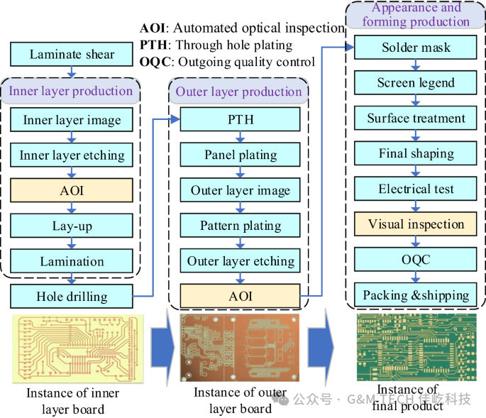
Schematic diagram of PCB manufacturing process
Source: Shows the overall process of PCB manufacturing, which includes the etching steps for both inner and outer layers, where the application of ferric chloride is key.
STEP
2
Etching Process Parameters and Optimization
Etching rate and quality are important factors affecting PCB performance, influenced by various parameters including etching solution concentration, temperature, pH, and the relative flow rate of the workpiece.
Etching solution concentration:In studies of low carbon steel etching, a ferric chloride concentration of 220 g/L achieved good etching results. In PCB copper etching, an appropriate FeCl₃ concentration is crucial for maintaining efficient and uniform etching.
Etching temperature:Increasing the etching temperature can accelerate the reaction rate, but in specific studies, 45°C is considered the relatively optimal temperature for low carbon steel etching. For copper etching, it is also necessary to operate within a certain temperature range to ensure etching efficiency and quality.
Stirring and flow rate:Stirring of the etching solution or movement of the workpiece (such as 50 RPM in low carbon steel etching, corresponding to a relative flow rate of 3.6 m/min) can promote the diffusion of reactants and products, thereby improving the uniformity and rate of etching. In the wet etching of micro copper PCB traces, applying air pressure can enhance etching results.
pH value:In low carbon steel etching, a pH value of 1.0 is considered one of the optimal conditions. For ferric chloride copper etching, the pH of the etching solution also affects its activity and selectivity.
Etching depth and precision:Ferric chloride etching can achieve uniform etching thickness, which is crucial for obtaining precise circuit patterns.
STEP
3
Advantages and Limitations of Ferric Chloride Etching
Advantages
Cost-effectiveness:The preparation of ferric chloride solution is simple and low-cost, making it very suitable for laboratory prototyping and small batch production.
Ease of operation:Compared to some complex industrial etching methods, the ferric chloride etching method is relatively simple to operate, making it accessible for electronics enthusiasts and educational practices.
Wide application:In addition to PCB manufacturing, ferric chloride etching is also used in the production of microfluidic channels, capacitive humidity sensors, and micro-electromechanical systems (MEMS) devices.
Limitations
Control of etching rate:Although ferric chloride has good etching effects, its etching rate can vary over time as the active FeCl₃ concentration decreases, while FeCl₂ and CuCl₂ are formed. This makes precise control of the etching process challenging, potentially leading to rough edges or undercutting of the traces.
Waste liquid treatment:The etching process generates waste liquid containing copper ions, which poses environmental pollution risks and requires proper treatment and recycling.
Regeneration issues:The regeneration of discarded ferric chloride etching solution is an important research area. Some studies have proposed electrolytic regeneration methods that can recover copper while regenerating the etching solution. For example, a carbon felt three-dimensional anode can be used to oxidize cuprous ions, avoiding the precipitation of oxygen and chlorine gas, while copper is recovered at the cathode. Biological regeneration methods are also being explored, where microorganisms oxidize ferrous ions back to ferric ions, achieving recycling of the etching solution and copper recovery.
STEP
4
Surface Treatment and Quality Control After Etching
After etching, PCBs typically require cleaning to remove residual etchant and resist. The cleaned boards will undergo further processes such as applying solder mask, silkscreen, surface treatment (to improve solderability and corrosion resistance), and final shaping and electrical testing. Quality control steps, such as automated optical inspection (AOI) and final visual inspection, are crucial for ensuring the reliability and performance of the PCBs.
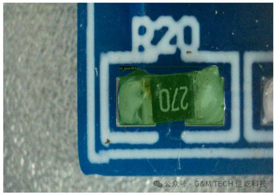
Image of circuit board defects
Source: Shows a small electronic component on a PCB with signs of wear or contamination on the surface. This emphasizes the importance of detecting and controlling surface defects during manufacturing and handling, as the quality of the etching process directly affects the reliability of the final product.
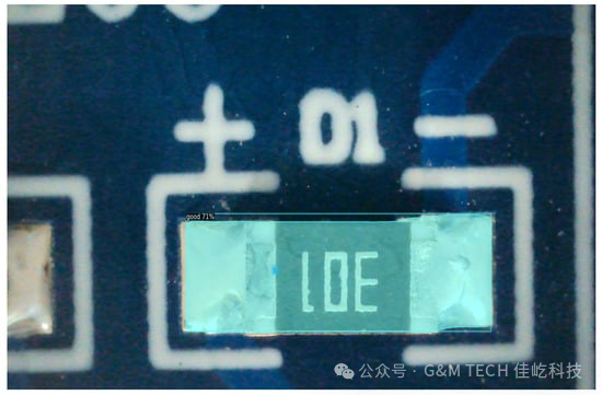
Close-up view of the circuit board
Source: Displays a close-up view of the circuit board with polarity markings and component identifiers, illustrating the need for fine patterns and clear markings in PCB manufacturing, all of which rely on high-quality etching processes.
STEP
5
Other Etching Technologies
In addition to ferric chloride wet etching, there are other etching technologies used in PCB manufacturing:
Laser etching:Industrial PCB manufacturers may use laser cutting or computer numerical control milling to form circuit paths, which is often more efficient than traditional methods but may risk damaging the circuit board.
Copper chloride etching:Copper chloride is another commonly used etchant, favored for its high etching rate and ease of regeneration.
Ammoniac copper etching:Ammoniac copper etching solution is also used in PCB production, and its composition optimization is crucial for forming conductive patterns.
Dry etching:Techniques such as deep reactive ion etching (DRIE) are primarily used for micro-nano processing of silicon materials, achieving extremely high aspect ratios and precise sidewall control. Although less directly related to PCB manufacturing, they represent the forefront of etching technology in microelectronics manufacturing.
Ferric chloride, as a classic and cost-effective etchant, plays an irreplaceable role in printed circuit board manufacturing. Despite challenges such as waste liquid treatment and etching rate control, the prospects for its application in PCB and related micro-device manufacturing remain broad through process optimization and advancements in etching solution regeneration technologies.

Jia Yi Technology

Official Website | gmtechcn.com
Sales Department Email | sale@gmtechcn