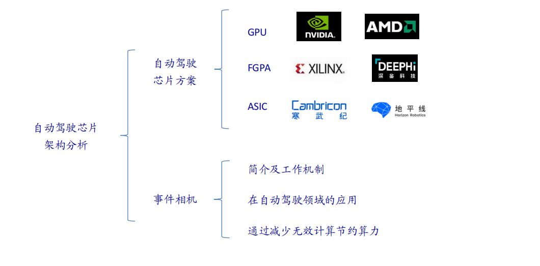
Comparison of Mainstream Architecture Solutions: Three Mainstream Architectures
The current mainstream AI chips can be mainly divided into three categories: GPU, FPGA, and ASIC. Both GPU and FPGA are relatively mature chip architectures in the early stage and belong to general-purpose chips. ASIC is a chip customized for specific AI scenarios. It has been confirmed in the industry that CPU is not suitable for AI computation, but it is still indispensable in the field of AI applications.
01
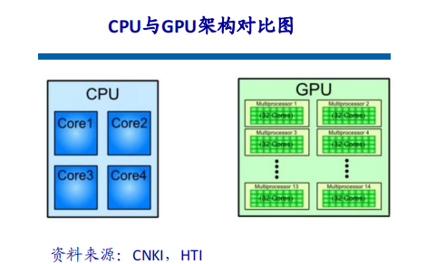
GPU SolutionComparison Between GPU and CPU Architectures The CPU follows the von Neumann architecture, which focuses on storing programs/data and executing them sequentially. Therefore, the CPU architecture requires a large amount of space to accommodate storage units (Cache) and control units (Control), while the computing units (ALU) occupy only a small portion. This limits the CPU’s capability for large-scale parallel computing, making it more adept at handling logical control. The GPU (Graphics Processing Unit) is a large-scale parallel computing architecture composed of numerous computing units, originally derived from the CPU specifically for processing image parallel computing data, designed to handle multiple parallel computing tasks simultaneously. The GPU also includes basic computing units, control units, and storage units, but its architecture differs significantly from that of the CPU, as shown in the architecture diagram below. Compared to the CPU, less than 20% of the CPU chip space is ALU, while over 80% of the GPU chip space is ALU. This means that the GPU has more ALUs for data parallel processing.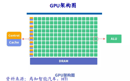 Differences Between GPU and CPU The CPU consists of several cores optimized for sequential processing, while the GPU has a large-scale parallel computing architecture composed of thousands of smaller, more efficient cores designed for simultaneous processing of multiple tasks. The significant differences between CPU and GPU arise from their design objectives, targeting two distinct application scenarios. The CPU requires strong versatility to handle various data types, while logical judgments introduce a significant number of branch jumps and interrupts, complicating its internal structure. In contrast, the GPU faces highly uniform, independent large-scale data and operates in a clean computational environment without interruptions.
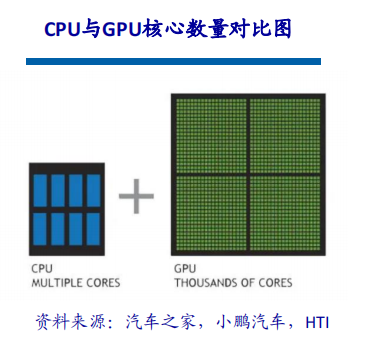 Overview of GPU Acceleration Technology For deep learning, hardware acceleration mainly relies on using Graphics Processing Units. Compared to traditional CPUs, the core computing power of GPUs is several orders of magnitude higher and more conducive to parallel computing. The multi-core architecture of GPUs contains thousands of stream processors that can execute computations in parallel, significantly reducing model computation time. As companies like NVIDIA and AMD continue to advance their GPU’s large-scale parallel architecture support, general-purpose GPUs have become an essential means to accelerate parallel applications. Currently, GPUs have reached a relatively mature stage. Using GPUs to train deep neural networks can fully leverage their efficient parallel computing capabilities with thousands of computing cores, significantly shortening the time required in scenarios with massive training data and occupying fewer servers. With appropriate optimization for suitable deep neural networks, a single GPU card can equate to the computing power of dozens or even hundreds of CPU servers, making GPUs the preferred solution in the industry for training deep learning models.
 When the scale of the trained model is relatively large, the training can be accelerated through data parallelism, which involves splitting the training data and using multiple model instances to train multiple chunks of data simultaneously. In implementing data parallelism, since the same model is trained with different data, the bottleneck affecting model performance lies in the parameter exchange between multiple CPUs or GPUs. According to the parameter update formula, all gradients computed by the models need to be submitted to the parameter server and updated accordingly, so the division of data chunks and the bandwidth to the parameter server may become bottlenecks limiting the efficiency of data parallelism. Besides data parallelism, model parallelism can also be used to accelerate model training. Model parallelism refers to splitting a large model into several fragments, with several training units holding them, and collaborating to complete the training of the large model.
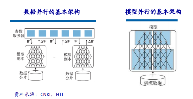 GPU Accelerated Computing GPU accelerated computing refers to the simultaneous use of Graphics Processing Units (GPU) and CPUs to speed up the execution of scientific, analytical, engineering, consumer, and enterprise applications. The GPU accelerator was first introduced by NVIDIA in 2007 and has since supported high-efficiency data centers for government labs, universities, companies, and small to medium-sized enterprises worldwide. GPUs can accelerate applications across platforms ranging from cars, smartphones, and tablets to drones and robots. GPU accelerated computing can provide extraordinary application performance by offloading the computationally intensive portions of applications to GPUs while the CPU runs the remaining program code. From a user’s perspective, the speed of application execution is significantly increased. Currently, GPUs are primarily focused on parallel matrix multiplication and addition, while the construction of neural network models and data flow transmission still occurs on CPUs. The interaction process between CPU and GPU includes: obtaining GPU information, configuring GPU id, loading neuron parameters to the GPU, GPU accelerating neural network computation, and receiving GPU computation results.
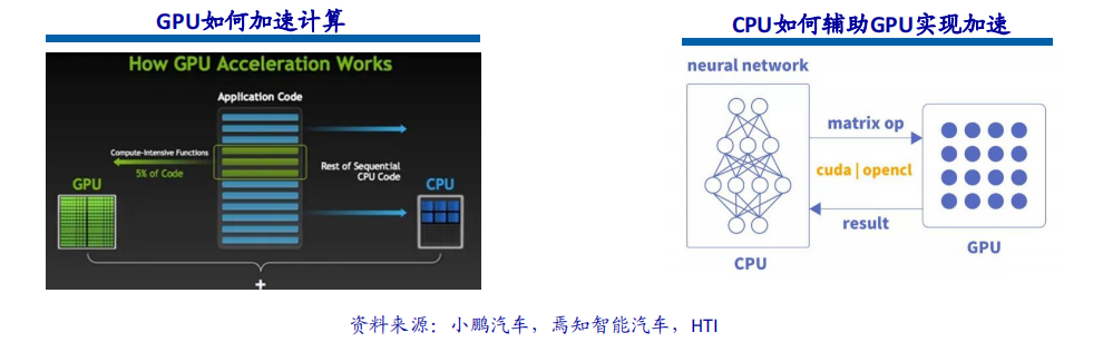 Why GPUs Are So Important in the Autonomous Driving Field One of the most critical technological domains in autonomous driving is deep learning. AI based on deep learning architectures is now widely applied in various fields of the automotive industry, including computer vision, natural language processing, sensor fusion, target recognition, and autonomous driving. From autonomous driving startups to internet companies and major OEM manufacturers, all are actively exploring how to utilize GPUs to build neural networks to achieve ultimate autonomous driving. Since the advent of GPU accelerated computing, it has provided a multi-core parallel computing architecture for enterprise data, supporting data sources that previous CPU architectures could not handle. Comparatively, to complete the same deep learning training tasks, the cost of using GPU computing clusters is only one two-hundredth of that of CPU computing clusters.
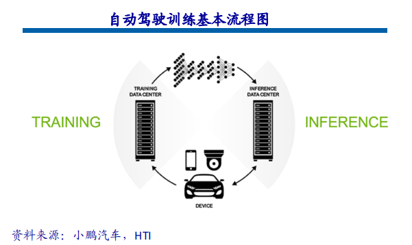 GPUs Are the Key to Autonomous Driving and Deep Learning Whether enabling cars to perceive their surrounding environment in real-time or quickly plan driving routes and actions, these tasks rely on the rapid response of the car’s brain, posing a significant challenge to computer hardware manufacturers. The process of autonomous driving constantly requires deep learning or AI algorithms to handle infinite possible situations, and the vigorous development of AI, deep learning, and autonomous driving has ushered in a golden era for GPU computing. Another important parameter of GPUs is floating-point computing power. Floating-point counting uses floating-point representation with varying lengths of binary to represent a number, as opposed to fixed-point numbers. High precision is required during the iterative process of autonomous driving algorithms, necessitating support for floating-point operations.
02
FPGA SolutionDefinition and Structure of FPGA Chips FPGA (Field-Programmable Gate Array) is a product developed further on the basis of programmable devices such as PAL, GAL, and CPLD. It appears as a semi-custom circuit in the field of application-specific integrated circuits, solving the shortcomings of custom circuits and overcoming the limitations of the number of gate circuits in existing programmable devices. FPGA chips are mainly composed of six parts: programmable input/output units, basic programmable logic units, complete clock management, embedded block RAM, rich routing resources, embedded lower-level functional units, and embedded dedicated hardware modules. Currently, mainstream FPGAs are still based on lookup table technology, far exceeding the basic performance of previous versions while integrating commonly used functions (such as RAM, clock management, and DSP) into hard-core (ASIC-type) modules.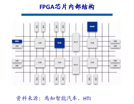 Working Principle of FPGA Since FPGA needs to be repeatedly reprogrammed, its basic structure for implementing combinational logic cannot be completed like ASICs through fixed NAND gates, but must adopt a structure that is easily reconfigurable. Lookup tables can meet this requirement well, and currently, mainstream FPGAs use SRAM-based lookup table structures, while some military and aerospace-grade FPGAs adopt Flash or fuse-and-re-fuse-based lookup table structures. Reconfiguration of the FPGA is achieved by changing the contents of the lookup table through programming files. The lookup table (Look-Up Table) is abbreviated as LUT, which is essentially a RAM. Currently, FPGAs often use 4-input LUTs, so each LUT can be considered a RAM with 4 address lines. When users describe a logic circuit through schematics or HDL language, the PLD/FPGA development software automatically calculates all possible results of the logic circuit and pre-writes the truth table (i.e., results) into RAM, allowing each input signal for logical operations to effectively input an address to look up the corresponding content and output it.
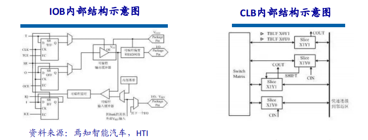
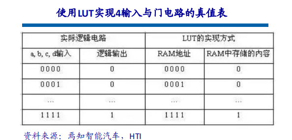 The programmable input/output units, abbreviated as I/O units, serve as the interface between the chip and external circuits, fulfilling the driving and matching requirements for input/output signals under different electrical characteristics. The I/O within the FPGA is categorized into groups, with each group independently supporting different I/O standards. Through flexible software configuration, it can adapt to various electrical standards and I/O physical characteristics, adjust the driving current, and change pull-up and pull-down resistors. Currently, the frequency of I/O ports is also increasing, with some high-end FPGAs supporting data rates of up to 2Gbps through DDR register technology. CLB is the basic logic unit within the FPGA. The actual number and characteristics of CLBs will vary depending on the device, but each CLB contains a configurable switch matrix, which consists of 4 or 6 inputs, some selection circuits (such as multiplexers), and flip-flops. The switch matrix is highly flexible and can be configured to handle combinational logic, shift registers, or RAM. In Xilinx’s FPGA devices, CLBs are composed of multiple (generally 4 or 2) identical slices and additional logic. Each CLB module can be configured for combinational logic, sequential logic, distributed RAM, and distributed ROM.
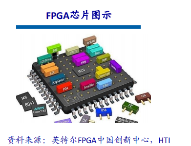
 FPGA: The “Chip” Killer of Autonomous Driving The autonomous driving and advanced driver assistance system (ADAS) sub-markets are undergoing transformation, posing new complex demands for computing and sensor capabilities. FPGA has unique advantages that other chip solutions cannot match, making it an excellent choice for meeting the evolving needs of the autonomous driving industry. FPGA is a special technology in the chip field, capable of repeatedly configuring through software tools while also possessing rich I/O interfaces and computing units. Therefore, FPGA can handle both pipeline parallelism and data parallelism according to specific application requirements, inherently offering advantages such as high computing performance, low latency, and low power consumption. FPGA features high throughput, high energy efficiency, and real-time processing capabilities, making it highly compatible with the technical requirements for autonomous driving. The standards and requirements for advanced driver assistance systems (ADAS) and in-vehicle experiences (IVE) are rapidly evolving, with system designers focusing on outstanding flexibility and faster development cycles while maintaining a higher performance-to-power ratio. By combining reprogrammable FPGAs with an increasing number of automotive-grade products, automotive designers can meet design requirements and stay ahead in the ever-changing automotive industry.
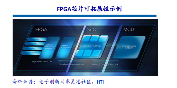
 More Adaptable Platforms For autonomous driving chips, true value lies in the utilization of the computing engine, that is, the difference between theoretical performance and actual performance. FPGAs contain a large number of routing links and small storage units. This combination allows designers to create custom data feed networks for their computing engines, achieving higher utilization levels. Programmable logic provides customers with high flexibility to adapt to the ever-changing demands of emerging application areas such as ADAS and autonomous driving. Utilizing improved interface standards, algorithm innovations, and new sensor technologies requires adaptable platforms that can support not only software changes but also hardware changes, which is precisely the advantage of FPGA chips. FPGA chips have scalability. Scalable chips change the number of programmable logic elements, mostly adopting pin-compatible packages. This means that developers can create a single ECU platform to house low, medium, and high versions of ADAS function packages and scale costs as needed by selecting the minimum density chip required.
 Differentiated Solutions FPGA chips allow developers to create unique differentiated processing solutions optimized for specific applications or sensors. This is unattainable for ASSP chips, even for those that provide dedicated accelerators, whose usage is limited and essentially available to all competitors. For example, Xilinx’s long-term customers have created high-value IP libraries accessible only to them, and these functions can be utilized across various products of the company. Since the 90nm node, Xilinx’s chips have been highly cost-effective for high-volume automotive applications, with over 160 million Xilinx chips applied in the industry.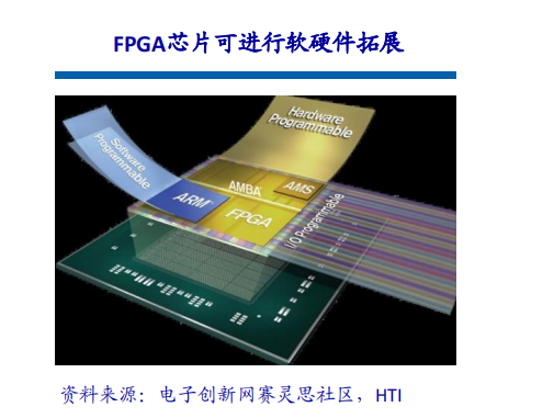
03
ASIC SolutionDefinition and Characteristics of ASIC ASIC chips can be categorized based on different terminal functions into TPU chips, DPU chips, and NPU chips. Among them, TPU stands for Tensor Processing Unit, specifically designed for machine learning. For instance, Google developed a programmable AI accelerator for the Tensorflow platform in May 2016, which can operate its internal instruction set when the Tensorflow program changes or updates algorithms. DPU stands for Data Processing Unit, which provides engines for computing scenarios such as data centers. NPU is a Neural Processing Unit, simulating human neurons and synapses at the circuit level and directly processing large-scale electronic neuron and synapse data with deep learning instruction sets. ASICs can be designed in fully customized or semi-customized ways. Fully customized designs rely on significant manpower and time investment to complete the entire integrated circuit design process autonomously. Although fully customized ASICs are more flexible and perform better than semi-customized ones, their development efficiency is considerably lower.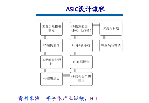 Significant Performance Improvement ASIC chips are highly suitable for AI application scenarios. For example, NVIDIA’s first chip designed from scratch for deep learning, the Tesla P100, has a data processing speed 12 times that of its GPU series launched in 2014. Google’s custom chip TPU for machine learning has elevated hardware performance to a level equivalent to that of current chips seven years after Moore’s Law development. Just as CPUs transformed massive computers in the past, AI ASIC chips will significantly change the landscape of today’s AI hardware devices. For instance, the renowned AlphaGo utilized around 170 GPUs and 1200 CPUs, requiring a server room and high-power air conditioning, along with multiple experts for system maintenance. However, if entirely using dedicated chips, it would likely only need the space of an ordinary storage box, with significantly reduced power consumption. The ASIC technology route is limited and open, requiring chip companies to develop towards mainstream networks, models, and operators related to driving. Under the same performance conditions, ASIC chips have smaller areas, lower costs, and lower power consumption. The future potential of the ASIC technology route is vast; choosing the ASIC route does not mean developing different ASICs for different vehicle models or conducting different validations. This is because the functions required for different vehicle models are generally similar, and chips can be limitedly open to models and operators, allowing rapid algorithm iteration without affecting the chip’s support for upper-layer functions. Collaborating with car manufacturers and chip design companies for differentiated customization is a better choice. Even with differentiated customization, 50% of the chip’s internal components are still generic. Chip design companies can perform differentiated designs based on existing versions to achieve partial differentiated functions.
04
Comparison of Mainstream Architecture Solutions: Three Mainstream ArchitecturesFPGA is a product developed further on the basis of programmable devices such as PAL and GAL. It appears as a semi-custom circuit in the field of application-specific integrated circuits, solving the shortcomings of custom circuits and overcoming the limitations of the number of gate circuits in existing programmable devices. Advantages: can be programmed infinitely, has low latency, supports both pipeline and data parallelism, with the strongest real-time capabilities and highest flexibility. Disadvantages: high development difficulty, only suitable for fixed-point operations, and relatively expensive. Graphics Processing Unit (GPU) is a microprocessor specifically designed for performing image and graphics-related computations on personal computers, workstations, game consoles, and some mobile devices (such as tablets and smartphones). Advantages: provides the foundation for multi-core parallel computing, with an extremely high number of cores supporting extensive data parallel computing and higher floating-point computation capabilities. Disadvantages: management control capability (weakest) and power consumption (highest).ASIC refers to application-specific integrated circuits designed and manufactured to meet the specific requirements of specific users and electronic systems. Currently, using CPLD (Complex Programmable Logic Device) and FPGA (Field-Programmable Gate Array) for ASIC design is one of the most popular methods. Advantages: as a product closely integrated with integrated circuit technology and specific users’ system technology, it has advantages such as smaller size, lighter weight, lower power consumption, improved reliability, enhanced performance, increased confidentiality, and reduced costs compared to general integrated circuits. Disadvantages: insufficient flexibility, and costs are higher than FPGA.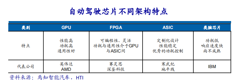
The Limitations of Power Theory: TOPS Performance Does Not Fully Equal Actual Performance
With the rise of ADAS and autonomous driving technologies, as well as the gradual deepening of software-defined vehicles, the demand for computing power and massive data processing capabilities in smart cars has surged, making traditional automotive chip “stacking” solutions insufficient to meet the computing power demands of autonomous driving. Ultimately, chips serve the vehicle computing platform of car manufacturers, and in the context of “software-defined vehicles,” addressing the support issues for intelligent driving system computing platforms cannot be achieved solely through chip power stacking. Chips are the stage for software, and the criteria for evaluating chip quality depend on whether the software above the chip can maximize its potential. The chip that enables software to run more efficiently is the “good chip” when comparing two chips with the same power. The most significant factors determining the true value of computing power are memory (SRAM and DRAM) bandwidth, actual operating frequency (i.e., supply voltage or temperature), and the batch size of algorithms. The TOPS computing power of a single chip is a key indicator but not the only one. Autonomous driving is a complex system requiring collaboration among vehicles, roads, clouds, and edges. Therefore, its competition involves not only chips but also hardware-software collaboration, platforms, and toolchains. The infinite expansion of chip computing power and embedded hardware will not be the future trend; hardware must also match reality. High power consumption and low utilization rates are issues behind high performance.
05
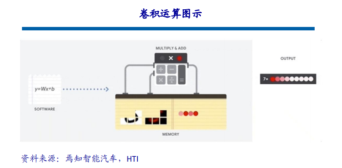
Introduction to Event CamerasOverview and Working Mechanism Event cameras are inspired by human and animal vision and are sometimes referred to as silicon retinas. Biological vision is sensitive only to changing areas, and event cameras capture the occurrence or change of events. In traditional vision fields, the information returned by cameras is synchronized; that is, at a specific time t, the camera will expose and fill all pixels at that moment into a matrix for return, generating a photograph. All pixels on a photo correspond to the same moment. As for video, it is merely a series of images, where the time intervals between adjacent images can vary, referred to as frame rate (frame rate) or time latency (time latency). Event cameras, similar to the human brain and eyes, skip irrelevant backgrounds and directly perceive the core of a scene, creating pure events rather than data. The working mechanism of event cameras is that when the brightness at a specific pixel location changes beyond a certain threshold, the camera will return an event in the aforementioned format, with the first two items representing the pixel coordinates of the event, the third item being the timestamp of the event, and the last item taking values for polarity (polarity) 0, 1 (or -1, 1), indicating whether the brightness changes from low to high or from high to low. Thus, within the entire camera’s field of view, as long as there is a change in pixel value, an event will be returned, and all these events occur asynchronously (no matter how small the time interval, they cannot happen simultaneously), so the timestamps of the events are different. Due to its simple return mechanism, it possesses low latency characteristics compared to traditional cameras, capturing pixel changes within very short time intervals, with delays at the microsecond level.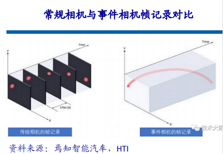 Applications in Autonomous Driving The visual recognition algorithms currently employed in the autonomous driving field are primarily based on convolutional neural networks. The computation of visual algorithms fundamentally involves repeated convolution operations. This computation is not complex, essentially involving addition, subtraction, multiplication, and division—essentially a product accumulation operation. However, this simple computation is prevalent in convolutional neural networks, which places high demands on processor performance. For instance, ResNet-152 is a 152-layer convolutional neural network that requires approximately 22.6 billion operations to process a 224*224 size image. If this network processes a 1080P camera at 30 frames per second, it requires as much as 33 trillion operations per second, which is quite significant.
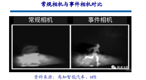
 Saving Computing Power by Reducing Ineffective Computations In the autonomous driving field, 99% of visual data in AI processing is useless background. For example, when detecting a ghost probe, the changing area is a small part, but traditional visual processing still has to handle 99% of the unchanged background area, wasting substantial computing power and time. Alternatively, like a diamond in a pile of sand, AI chips and traditional cameras need to identify every grain of sand to locate the diamond, while humans can detect the diamond with just a glance. The time consumed by AI chips and traditional cameras is 100 to 1000 times that of humans. In addition to reducing redundant information and having almost no latency, the advantages of event cameras include low latency, which prevents blurring when capturing high-speed objects. Traditional cameras may experience blurring due to exposure time, whereas event cameras do not. Additionally, event cameras possess true high dynamic range; due to their characteristics, traditional cameras will “go blind” in environments with strong or weak light, but pixel changes still exist, allowing event cameras to see what is in front of them.
 Welcome to All Automotive Industry Chain (Including Electrification Industry Chain) Angel Round and A Round Enterprises to Join the Group (Friendly connections with 700 automotive investment institutions, including top-tier organizations; A selection of high-quality projects will be presented to existing institutions by theme); There are communication groups led by sci-tech innovation company leaders, covering dozens of groups in automotive manufacturing, automotive semiconductors, key components, new energy vehicles, intelligent connected vehicles, aftermarket, automotive investment, autonomous driving, vehicle networking, etc. Please scan the administrator’s WeChat to join the group (Please indicate your company name).