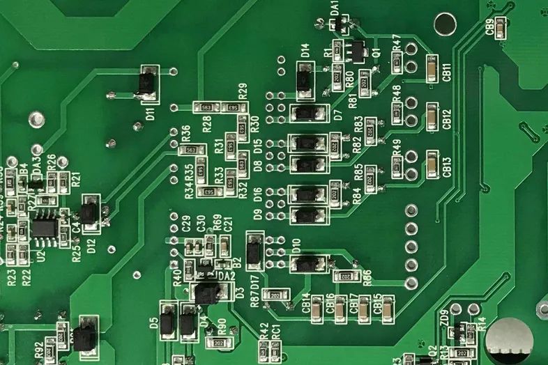
The main purpose of PCB Surface Finish is to protect the underlying copper layer from oxidation to ensure good soldering and electrical conductivity, and to continuously protect the solder joints from further oxidation after soldering. Below is a brief introduction to the advantages and disadvantages of common PCB surface treatment processes.

1. Bare Copper Board
Advantages: Low cost, smooth surface, good solderability (when not oxidized).
Disadvantages: Easily affected by acid and humidity, cannot be stored for long, must be used within 2 hours after unsealing because exposed copper easily oxidizes; cannot be used for double-sided boards, as the second side oxidizes after the first reflow soldering. If there are test points, solder paste must be added to prevent oxidation, otherwise, subsequent contact with the probe will be poor.
2. OSP Process Board
OSP differs from other surface treatment processes in that it acts as a barrier layer between copper and air. In simple terms, OSP is a chemical method that grows a layer of organic film on a clean bare copper surface. The only function of this organic film is to ensure that the inner copper foil does not oxidize before soldering. When heated during soldering, this layer evaporates, allowing solder to join copper wires and components together. However, this organic film is not very corrosion-resistant; an OSP circuit board exposed to air for about ten days cannot have components soldered onto it. Since it is organic and not metallic, it is cheaper than tin plating.
Advantages: Retains all the advantages of bare copper board soldering; expired boards can be reprocessed.
Disadvantages: 1. OSP is transparent and colorless, making it difficult to inspect and determine if it has been treated with OSP.
2. OSP itself is insulating and non-conductive, which affects electrical testing. Therefore, test points must have a stencil applied with solder paste to remove the original OSP layer for probe contact during electrical testing. OSP cannot be used as a treatment for electrical contact surfaces, such as keyboard surfaces.
3. OSP is easily affected by acid and temperature. When used for secondary reflow soldering, it must be completed within a certain timeframe; typically, the effect of the second reflow soldering is worse. If stored for more than three months, it must be reprocessed, and must be used within 24 hours after opening.
3. Gold Plated Board
Gold plating uses real gold; even a thin layer accounts for nearly 10% of the circuit board’s cost. Gold is used as a plating layer for ease of soldering and to prevent corrosion. Even after years of use, the gold fingers of memory modules remain shiny, while copper, aluminum, and iron would have rusted into scrap. Gold plating is widely used in solder pads, gold fingers, and connector springs on circuit boards.
Advantages: Strong conductivity, good oxidation resistance, and long lifespan. The plating is dense and relatively wear-resistant.
Disadvantages: Higher cost, poorer soldering strength.
4. ENIG (Electroless Nickel Immersion Gold)
ENIG, also known as nickel gold or immersion nickel gold, is a chemical method that wraps a thick layer of nickel-gold alloy with good electrical performance on the copper surface, providing long-term protection for PCBs. Unlike OSP, which only serves as a rust barrier, ENIG can be useful and achieve good electrical performance during the long-term use of PCBs. It also has environmental tolerance that other surface treatment processes lack.
Advantages: 1. The surface of PCBs treated with ENIG is very flat, with excellent coplanarity, suitable for key contact surfaces.
2. ENIG has excellent solderability; gold quickly integrates into molten solder, forming a Ni/Sn metallurgical compound with solder.
Disadvantages: The process is complex, and achieving good results requires strict control of process parameters. The most troublesome issue is that PCB surfaces treated with ENIG can easily develop black pad effects during ENIG or soldering processes. The black pad is directly manifested by excessive oxidation of Ni and too much gold, which can embrittle solder joints and affect reliability.
5. ENEPIG (Electroless Nickel Palladium Immersion Gold)
Compared to nickel gold, ENEPIG has an additional layer of palladium between nickel and gold. In the displacement reaction of gold deposition, the palladium layer protects the nickel layer from excessive corrosion by displaced gold, while preparing for immersion gold.
Advantages: It has a very wide range of applications, and the chemical nickel palladium gold surface treatment can effectively prevent reliability issues caused by black pad defects, making it a substitute for nickel gold.
Disadvantages: Although ENEPIG has many advantages, palladium is expensive and a scarce resource. Like nickel gold, it also requires strict process control.
6. Tin Plated Circuit Board
The silver-colored board is called a tin-plated board. A layer of tin is sprayed onto the outer layer of copper traces, which can also aid in soldering. However, it cannot provide long-term contact reliability like gold. It does not affect already soldered components, but for pads exposed to air for a long time, reliability is insufficient, such as grounding pads and spring sockets. Long-term use can easily lead to oxidation and rust, resulting in poor contact.
Advantages: Lower price, good soldering performance.
Disadvantages: Not suitable for soldering fine-pitch pins and small components, as the surface flatness of tin-plated boards is relatively poor. During PCB processing, solder balls can easily form, which can cause short circuits for fine-pitch components. In double-sided SMT processes, because the second side has already undergone high-temperature reflow soldering, it is very easy for the tin plating to remelt, causing solder balls or droplet-like solder points due to gravity, resulting in an even less flat surface, thus affecting soldering issues.
7. Silver Immersion
Silver immersion is a process that lies between OSP and chemical nickel/gold immersion, characterized by simplicity and speed. Silver immersion is a displacement reaction, coating nearly submicron-level pure silver. Sometimes, the silver immersion process includes some organic substances, mainly to prevent silver corrosion and eliminate silver migration issues; this thin layer of organic matter is generally difficult to measure, with analyses showing the organic weight is less than 1%. Even when exposed to hot, humid, and polluted environments, it still provides good electrical performance and maintains good solderability, although it loses its luster. Since there is no nickel beneath the silver layer, silver immersion does not possess the good physical strength of chemical nickel/gold.
Advantages: The soldering surface of silver immersion has good solderability, excellent coplanarity, and does not have the conductive barrier issues of OSP; however, its strength is not as good as gold when used as a contact surface (e.g., key surfaces).
Disadvantages: A significant issue with silver immersion is the migration of silver electrons; when exposed to humid environments, silver can migrate under voltage. Adding organic components to silver can reduce the electron migration issue.
8. Hot Air Solder Leveling (HASL)
Since all solder materials are tin-based, the tin layer can match any type of solder. However, previous PCB processes using HASL were prone to tin whiskers, and during soldering, tin whiskers and migration could lead to reliability issues, limiting the adoption of HASL. Later, organic additives were added to the HASL solution, allowing the tin layer structure to form a granular structure, overcoming previous issues, and providing good thermal stability and solderability. The biggest weakness of HASL is its short lifespan, especially when stored in high-temperature and high-humidity environments, where the Cu/Sn intermetallic compound will continue to grow until it loses solderability.
Disadvantages: The biggest weakness of HASL is its short lifespan, especially when stored in high-temperature and high-humidity environments, where the Cu/Sn intermetallic compound will continue to grow until it loses solderability. Unlike the diffusion issues of chemical nickel/gold, HASL boards cannot be stored for too long.


Some Electronic Book Screenshots

