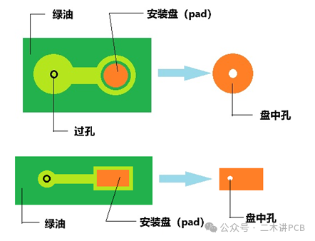
To achieve high-density wiring, shorten signal transmission paths, and enhance signal integrity, the via in pad is introduced. However, the design of vias in pads presents challenges for soldering. Since the vias are located within the pads, some solder may flow into the vias during the soldering process, leading to insufficient solder on the pads, resulting in cold solder joints, low solder joint strength, and poor fatigue resistance.To address the soldering issues caused by vias in pads, the optimal solution is to fill the vias and then cover the filled material (insulating resin or high thermal conductivity metal paste) with a layer of copper, which is known as the plating over filled via (POFV).

Illustration of Via in Pad
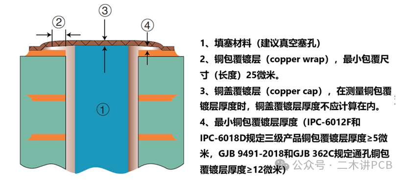
Key structural indicators of POFV include the thickness of the copper coating, the thickness of the copper cap layer, the coating length, protrusions, depressions, and voids in the filled vias.
The copper wrap: This copper layer has a wrapping morphology, extending continuously from the inner wall of the via to the surface of the PCB at the corners (excluding the copper layer on the via wall). When there are width requirements, the copper wrap should extend at least 25 microns (as shown in the size marked ② in the figure).

The copper cap: This layer acts as a “cap” over the filled material, providing a larger mounting area or heat dissipation area. Voids in the copper cap layer are not allowed, and separation from the bottom coating is not permitted, although separation between the copper cap layer and the filled material is allowed.

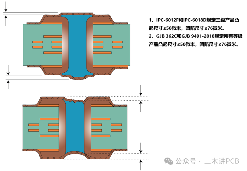
Protrusions and depressions: The swelling or shrinking of the filled material during curing or subsequent processes such as grinding, etching, and leveling may cause protrusions and depressions in POFV. Currently, both domestic and international standards have very lenient regulations on protrusion and depression values, making them unsuitable for applications such as bare die bonding or soldering. Therefore, this indicator is generally determined through AABUS (as agreed between user and supplier).

Protrusions and Depressions in POFV Structure
Voids in Fill Material: Traditional silk-screen filling (at normal pressure) or vacuum filling can be used. Voids in the fill material are actually bubbles trapped in the fill material that form during curing when the bubbles do not escape. Voids are allowed within the vias, and the fill material should occupy more than 60% of the volume of the via (as per IPC 6012F and IPC 6018D regulations for level 2 and level 3 products). However, in practical applications, to ensure the reliability of high-temperature assembly or stacked vias, visible voids are generally not permitted.