 With the continuous expansion of the 10.5 generation LCD and 6th generation flexible AMOLED production lines, the application of touch screens has also been continuously expanded. Currently, display panels are showing two major development trends: one is ultra-large size, and the other is curved and foldable. These two major trends have raised new requirements for touch screens, such as fast response, precise control, and flexibility. Therefore, various companies are accelerating the development of new materials to try to seize the leading edge, and SNW, which possesses both advantages, is beginning to emerge in the display field.
Concept and Process Technology of SNW
Silver nanowire is a nanomaterial with a diameter of 25~300nm and a length of 10~200um grown by chemical methods. In addition to having the excellent conductivity of silver, silver nanowires also have excellent light transmission and flexibility due to their nanoscale size effect. Therefore, they are regarded as the most likely material to replace traditional ITO transparent electrodes, providing possibilities for flexible and bendable LED displays and touch screens. Additionally, due to the large aspect ratio effect of silver nanowires, they also have outstanding advantages in applications such as conductive adhesives and thermal adhesives.
To be used in displays, it is necessary to first producesilver nanowire conductive films.Silver nanowire conductive films refer to high-tech products obtained by precision coating transparent silver nanowire ink on transparent organic film materials and curing. The conductivity and light transmission performance of the film vary depending on the coating density of the silver nanowire ink. Due to their good conductivityand light transmission performance, silver nanowire conductive films are particularly suitable for the production of touch screens.
The production process of silver nanowire TP mainly consists of laser engraving technology and photolithography technology.
Laser Engraving Process Flow
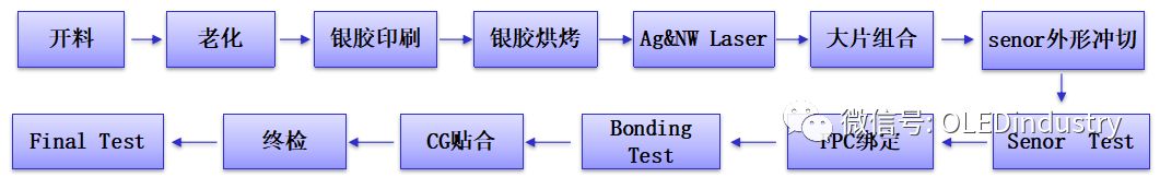
Challenges in Laser Engraving Process
1. Compatibility between silver nanowire conductive film and silver glue, ensuring conductivity and adhesion at the overlap.
2. Quality control of silver glue printing, ensuring uniform printing thickness without debris or voids.
3. Debugging of Ag&NW synchronous laser engraving process, especially for large size touch screens that involve multiple splicing, ensuring both appearance and functionality are OK.
Photolithography Process Flow
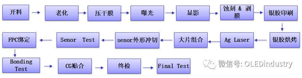
Challenges in Photolithography Process
1. Compatibility between silver nanowires, dry film, and etching solution, ensuring adhesion and resolution of dry film to silver nanowires and etching of silver nanowires and dry film by the etching solution.
2. Compatibility between silver nanowire conductive film and silver glue, ensuring conductivity and adhesion at the overlap.
Analysis of Touch Materials
Touch sensors have undergone a process of replacing glass with film. New flexible transparent conductive materials such as conductive polymers, silver nanowires, metal meshes, carbon nanotubes, and graphene have been rapidly developed and quickly commercialized in recent years. These materials have a strong potential to replace ITO transparent conductive films, especially in the medium to large size touch screen field.
From the cost analysis of upstream materials in the touch screen industry, ITO materials account for about 40%. With the development of the touch screen industry, the demand for ITO materials will continue to grow. As a rare metal, indium not only has a continuously rising price but also faces the risk of depletion. Therefore, the analysis of the touch materials in the current competitive landscape focuses on graphene, Metal Mesh, and silver nanowires as alternatives to ITO.
Analysis of Mainstream Technologies Replacing ITO
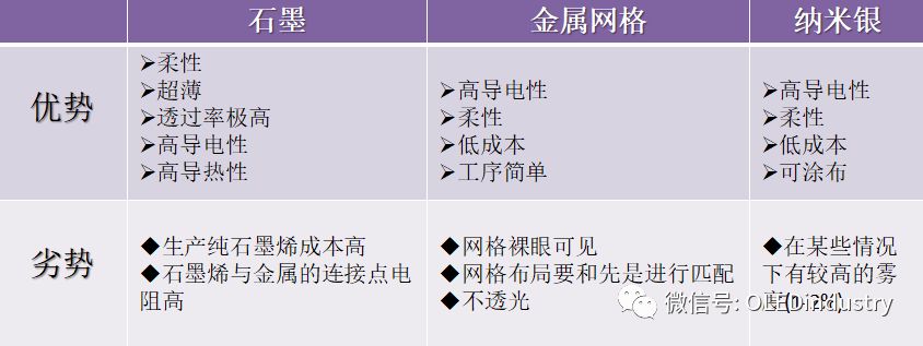
Graphene
Characteristics: Strength is 200 times that of steel, thickness is only one atomic diameter Advantages compared to traditional ITO:
1. First, the raw materials are relatively easy to obtain.
2. Flexibility is an important characteristic of graphene, and its bending performance is mainly limited by the bending limit of its substrate PET material.
3. Single-layer graphene has good light transmittance, absorbing only 2.3% of light.
4. Theoretical resistivity is low, even lower than that of copper/silver.
5. It also has multiple excellent properties such as high temperature resistance, waterproof, and corrosion resistance to alkali and salt.
Defects: Currently, the development of graphene touch screens is still in the early stages of the industry, but apart from upstream materials, the development of the downstream supply chain is still relatively slow, and yield rates need improvement. Therefore, large-scale commercial use is still some time away.
Metal Mesh
Characteristics: Metal mesh (Metal Mesh) is made of a conductive ink that is usually silver (Ag) or copper (Cu), and its shape looks like a barbecue grill made up of extremely thin metal wires.
Advantages over traditional ITO: The biggest advantage of metal mesh in touch sensors is that its impedance is less than 10 ohms, and its manufacturing cost is slightly lower than ITO, with better transparency and higher flexibility, making it applicable to laptops and PC panels of larger sizes.
Limitations: First, yield rates are unstable. Second, there are few companies capable of mass-producing Metal Mesh touch panels. Third, the cost of using Metal Mesh solutions with LCD panels can increase.
Silver Nanowires
Characteristics: Silver nanowire (SNW, silver nano wire) technology involves applying silver nanowire ink material onto plastic or glass substrates, and then using laser lithography technology to create a transparent conductive film with a nanometer-scale silver wire conductive network pattern.
Advantages: 1. Higher light transmittance; 2. Smaller bending radius with lower resistance change rate when bent; 3. More advantageous when applied to devices with curved displays, such as smartwatches and wristbands.
Defects: Silver nanowires exhibit irregular distribution, covering the entire surface of the glass substrate, leading to severe diffuse reflection, and haze issues are serious. The haze problem of the screen can cause strong reflections in outdoor lighting conditions, making it difficult for users to see the screen clearly.
Limitations of ITO,Prospective Analysis of SNW
From the cost analysis of upstream materials in the touch screen industry, ITO materials account for about 40%. With the development of the touch screen industry, the demand for ITO materials will continue to grow. As a rare metal, indium not only has a continuously rising price but also faces the risk of depletion, so the development of alternative materials such as graphene, Metal Mesh, and silver nanowires is closely monitored by the market.
New flexible transparent conductive materials such as conductive polymers, silver nanowires (metal mesh), carbon nanotubes, and graphene have been rapidly developed and commercialized in recent years. These materials have a strong potential to replace ITO transparent conductive films, especially in medium to large size touch screens.
Currently, the most widely used and demanded material remains ITO, but why develop new materials to replace ITO? Because ITO has its pros and cons. ITO has good light transmittance, low thickness, is easy to etch into electrode patterns, has high hardness, is wear-resistant, and even has good resistance when coated thicker. The insurmountable drawback of ITO is its high cost and significant initial fixed asset investment (approximately 35 million for large vacuum coating equipment lines, which is over 50% higher than the investment in silver nanowire coating equipment), and ITO is not conducive to producing curved screens. Most importantly, the raw material used in ITO is the rare metal indium, which has very low global reserves. With various countries implementing protective policies for rare earth resources, its cost has been continuously rising, and the usage of indium has been rapidly increasing since 2010. Additionally, recycling old electronic products containing ITO is difficult, indium is toxic, and the recycling cost is high. Therefore, ITO is not conducive to the popularization of the globally prevailing environmental protection concept.
In contrast, silver nanowires have a wide range of raw material sources, low raw material costs, excellent ductility, and are suitable for large-scale industrial production. In the upcoming flexible display era, silver nanowires have an irreplaceable position. With excellent ductility, a smaller bending radius, and a smaller resistance change rate when bent, they are more advantageous when applied to devices with curved displays, such as smartwatches and wristbands.
Additionally, currently, the transparent conductive material mainly used for small touch screens (below 10 inches) is indium tin oxide (ITO). ITO belongs to semiconductor materials, with mainstream specifications for ITO films having an impedance value of about 150 ohms (Ω)/unit area. This conductivity is sufficient for touch areas below 10 inches, but it is not suitable for medium, large, or ultra-large touch areas.Moreover, ITO is a metal ceramic, and when the touch area becomes curved or flexible, the brittleness of ITO can easily lead to a rapid increase in impedance value, resulting in poor impedance stability.
It is evident that ITO is not suitable for medium to large touch screens and flexible touch screens. Therefore, high conductivity and high flexibility solutions such as metal meshes and silver nanowires are accelerating industrialization and have already been applied to large size panels such as laptops and computers.
Analysis of SNW Market Applications
More Suitable for Large Size and Curved Screens
Compared to silver nanowires, the industrialization speed of metal meshes is faster.
Metal mesh utilizes metals like silver, copper, or oxides that are easy to obtain and low-cost raw materials to form conductive metal mesh patterns on PET and other plastic films. Its resistance can be as low as 0.1 ohms (Ω)/square inch, providing good touch performance. However, due to the limitations of printing technology, the metal wire width of the touch sensor patterns is relatively thick, and at high pixel densities, moiré interference patterns are very obvious. Therefore, it is not suitable for high-resolution products and is more suitable for medium-sized displays viewed from a distance, such as laptops and smart TVs.
Silver nanowires are applied by coating silver nanowire ink material onto plastic or glass substrates, followed by laser or photolithography to create transparent conductive films with a nanometer-scale silver wire conductive network pattern. The line width of silver nanowires is about 20nm, with no moiré interference issues, making them applicable to various sizes of displays. Additionally, silver nanowire films have a smaller bending radius than metal mesh films and exhibit lower resistance change rates when bent, making them more advantageous in applications for curved display devices.
Furthermore, in the large and ultra-large touch screen field, the cost of silver nanowires is only 1/5 of that of equivalent Japanese manufactured metal meshes.
The domestic market for silver nanowires and silver nanowire conductive inks is almost monopolized by Cambrios, and the high prices have slowed the industrialization pace of this technology.
Entering the Large Interactive Screen Market and Flexible Foldable OLED Markets
Currently, the industrialization speed of metal meshes is faster than that of silver nanowires and has been applied in medium-sized touch screen markets such as laptops. Therefore, starting from the large and ultra-large touch screen markets where silver nanowires have obvious advantages, it is gradually expanding into the medium-sized touch screen market.
On one side, the generations of LCD panels are continuously improving, with the gradual release of the 10.5 generation line; on the other side, with the continuous stable growth of the national economy and the acceleration of social development, the demand for commercial large screen display markets is increasing, and large screen display technology and markets are gradually developing, with growing demands in industries such as education, media, advertising, and conferences.
The timing for SNW to enter the large screen market has arrived, and with the increasingly obvious trend of flexible foldable AMOLED, SNW, due to its inherent flexible and foldable characteristics, has begun to slowly penetrate OLED flexible products.
If you want to learn more about opportunities for SNW in the flexible AMOLED era, you can attend the 2018 Polyimide Film Materials Technology and Application Forum tomorrow (July 4) to hear a speech by the leading company Cambrios on “CPI Based Silver Nanowire Transparent Conductive Film Technology” by General Manager Xiao Zhongqin.

Dr. Xiao Zhongqin is currently the CEO and General Manager of Cambrios Advanced Materials Technology Corporation. Dr. Xiao obtained his PhD in Chemical Engineering from National Tsing Hua University and worked at AU Optronics, responsible for research and development of oxide TFT, organic TFT, and R2R printing technology, while also serving as the head of multiple multinational cooperation projects in flexible panel technology applications.
In 2010, he joined Polyera Corporation, establishing Taiwan’s first flexible OTFT array experimental line, and in 2015 successfully broke through the yield bottleneck in manufacturing flexible displays on large-scale production equipment, launching the world’s first flexible display wearable product.
Cambrios Advanced Materials provides solutions for the consumer electronics market using silver nanowire technology based on its proprietary innovative technology.
The breakthrough transparent conductor products launched by Cambrios can simplify the manufacturing process of electronic devices, enhancing the performance of current and next-generation consumer devices while reducing costs, including applications in large area and flexible touch as well as other high-conductivity optical transparent applications.
The main products offered by Cambrios include: ClearOhm™ (silver nanowire ink): This coating material produces transparent conductive films through wet processes, with optical and electrical performance significantly higher than current materials such as indium tin oxide. Applications include transparent electrodes for touch screens, electromagnetic shielding, OLED displays, electronic paper, OLED lighting, and thin film optoelectronic devices.
Recommended Content

【@You 】2018 New Display AMOLED Industrialization Technology Summit Registration Channel Opened
Panel Array Process Brief and List of 84 Related Equipment Companies
China Star Optoelectronics: Second G11 line has been deployed, not in a hurry to build small-sized T5 factory
Analysis of AMOLED FMM Technology and the Real Global Situation
Overview of Mainstream AMOLED Manufacturers in Mainland China and the Coating Equipment They Use (Updated Version)