1. First, let’s discuss open-drain output and push-pull output
First, watch the video explanation:
The following video is from Guo Tianxiang
Push-Pull Output
- Structure and Principle: A push-pull output circuit consists of two complementary transistors (usually an NPN transistor and a PNP transistor). In this structure, when the input is high, the upper transistor (like the NPN) conducts, while the lower transistor is off, allowing current to flow from the power supply through the conducting transistor to the load, providing a high level to the load; when the input is low, the situation is reversed, the lower transistor (like the PNP) conducts, the upper transistor is off, and current flows from the load through the conducting transistor to ground, providing a low level to the load. Thus, through the alternating conduction and cutoff of the two transistors, it provides a complete level output to the load, akin to “push” and “pull”.
- Characteristics
- Strong Output Capability: It can provide a large driving current, capable of directly driving loads that require significant current, such as small relays, digital tubes, etc.
- Fast Response Speed: Due to the fast switching speed of the transistors, push-pull output can quickly switch between high and low levels, suitable for high-frequency signal output.
- Stable Levels: It can output stable high and low levels, with strong anti-interference capability.
- Application Scenarios: Commonly used in situations requiring strong driving capability and fast response speed, such as motor driving, audio power amplification, and high-speed transmission of digital signals.
Open-Drain Output
- Structure and Principle: In an open-drain output circuit, the drain (D pin) of the output transistor (usually an NMOS) is left floating, requiring an external pull-up resistor to function properly. When the input is high, the transistor is off, and the output is connected to the power supply through the pull-up resistor, presenting a high level; when the input is low, the transistor conducts, grounding the output, presenting a low level.
- Characteristics
- High Flexibility: By changing the connection method and resistance value of the pull-up resistor, it can flexibly adapt to different voltage requirements and load characteristics. For example, multiple open-drain output pins can be connected together, using a single pull-up resistor to achieve “wired AND” logic functionality.
- Applicable to Various Level Standards: Since the pull-up resistor can be connected to different power supply voltages, open-drain output can conveniently realize level conversion between different standards, facilitating interfacing with circuits of other voltage levels.
- Strong Sinking Current Capability: It can withstand a large sinking current, meaning when the output is low, it can absorb a significant amount of current.
- Application Scenarios: Commonly used in situations requiring “wired AND” logic, level conversion, and high sinking current requirements, such as I²C buses and certain sensor output interfaces.
From the perspective of active and passive, the differences between push-pull output and open-drain output are as follows:
- Push-Pull Output: It is an active output type. It can actively control the high and low levels of the output, directly driving the output pin to high or low based on the state of the input signal using the two complementary transistors. For example, when driving an LED, push-pull output can directly provide enough current to light the LED and can quickly control the LED’s on/off state without requiring additional external circuitry to determine the output state, demonstrating strong proactivity and driving capability.
- Open-Drain Output: Relatively, it is a passive output method. Open-drain output cannot actively output a high level; it relies on an external pull-up resistor to determine the high level state. When the transistor conducts, it can actively pull the output pin to low, but when outputting a high level, it is passive, depending on whether the external pull-up resistor is connected and the state of the connected power supply. For instance, on an I²C bus, multiple devices’ open-drain output pins are connected together, and each device cannot actively determine the high level state of the bus; only when all devices do not pull the bus low will the bus present a high level due to the action of the external pull-up resistor, reflecting the passivity of open-drain output when outputting a high level.
2. For IIC, to solve the short circuit problem, besides using open-drain, tri-state gates can also be used.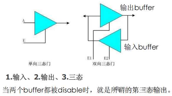
Now we understand why I2C must use open-drain with pull-up resistors. Next, let’s talk about the selection of pull-up resistors. There was once an I2C chip that could not be accessed at high temperatures, but everything was normal at room and low temperatures.
Here, let’s first consider a question: I2C is latch (level-triggered), not flip-flop (edge-triggered), so under normal circumstances, we do not care about the rising and falling edges. However, the problem lies here; our chip has requirements for the edges of SCL and SDA. Why is that?
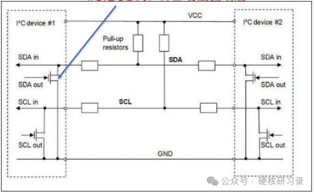
Look at the image below. When SDA outputs a high level, the red arrow indicates that VCC charges through the pull-up resistor and capacitor, while when SDA outputs a low level, the blue arrow indicates the opposite.
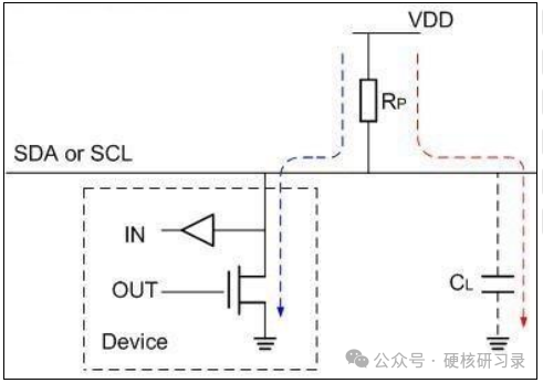
Where does this capacitor come from?
1) Stray capacitance from the traces
2) Input pin capacitance of the I2C chip
For convenience, we will use a single capacitor to represent this.
We can easily see that the output high is slower because of the resistance and capacitance blocking, requiring exponential charging through RC, while the output low is faster due to the MOS driving. Therefore, we will only study the rising edge.
Now, let’s answer why I2C has requirements for rise time? What problems arise if it is too slow? The I2C Fast Mode frequency is 3.4MHz, and the requirements for rise time become increasingly stringent with the increase in frequency (or rate).
If the SCL signal is fast enough, it will be the red signal; if too slow, it will be the blue signal.
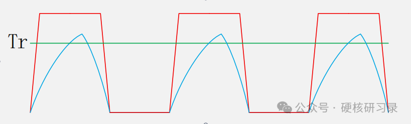
It is not difficult to see that the blue line crosses the green threshold too quickly, causing the receiver to fail to correctly identify the high level. Consequently, the receiver cannot correctly latch the data from SDA.
First, regarding the capacitance value: 1) It is affected by the board area, 2) The number of devices on the bus, 3) Traces, etc., with the input capacitance of the chip summed up, plus stray capacitance from the traces.
What we can actually change is the resistance. By appropriately adjusting the resistance value, we can achieve a reasonable rise time that meets the requirements of the receiving chip and provides a certain margin.
However, changing the resistance value requires careful calculation; it cannot be too small or too large, but rather reasonable.
Based on experience, the following can be used as a reference:
Generally, under a 5V power supply, pull-up resistors of 4.7kΩ or 5.1kΩ are commonly selected.In a 3.3V system, common choices include 2.2kΩ, 3.3kΩ, 4.7kΩ, etc. In some portable devices with high power consumption requirements, 4.7kΩ may be chosen to sacrifice some speed for lower power consumption; while in scenarios requiring high speed, 2.2kΩ or 3.3kΩ may be selected.3. Common Issues Encountered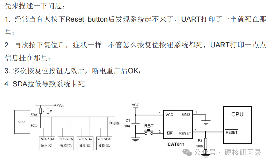
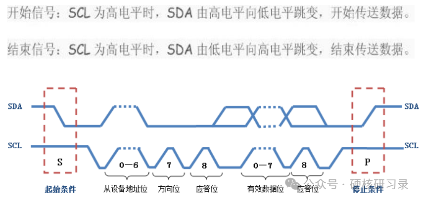 IIC defaults to high level due to the pull-up, so it is initially high. When data is transmitted, it is pulled low for signaling, thus transitioning from high to low indicates the start condition.Read/Write Timing:
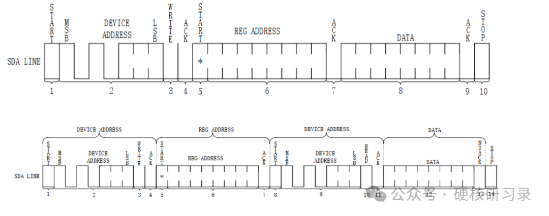 Generally, issues arise during reading, which can get stuck.
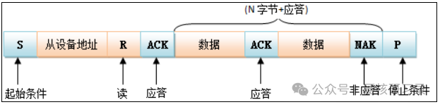
This is an I2C read operation, with the following sequence:
1. Master sends start;
2. Master sends address and read command;
3. Slave gives ACK and then sends data data7-0, a total of 8 bits driven by the slave on I2C SDA (SCL is always driven by the master), with a total time of 80us for 8 bits (assuming a rate of 100K, period of 10us).
If during this 80us time someone presses the reset button, what will happen?
The SDA data signal remains low, prompting software engineers to make the following modifications in the code:
1. When SDA is detected to be pulled low;
2. The software continuously sends 9 clock pulses;
3. During the 9 clock pulses, SDA will toggle high and low;
4. After the device has sent all data, SDA is released;
5. At this point, when the state machine reaches the NAK phase, SDA releases and goes high, generating a NAK;
6. Note that the 9 clock pulses may not be fully utilized; the EEPROM releases SDA upon reaching the NAK phase, but the CPU is unaware and continues to send all 9 clock pulses;
7. Finally, the CPU sends a stop to end the entire read operation;
Finally, resolving the issue