| Process Node | Technical Details | Results and Advantages | Application Areas |
|---|---|---|---|
| 90nm CMOS | 1. First to mass produce this technology on 300mm wafers.2. Developed three optimized process flows for manufacturing products with different requirements.3. Reduced transistor gate width to 37nm, allowing different threshold transistors to be placed on the same die.4. Utilized industry-leading (37nm) gate lengths, high-efficiency gate dielectric scaling, transistor channel conduction stress, nickel silicide to reduce gate resistance, and ultra-thin source/drain connections. | 1. Manufactured over 600 million devices with more than 60 different designs.2. Achieved single-chip mobile phone device delivery, driving the development of wireless handheld terminals.3. Tripled processing speed for voice, video, and data, saving one-third of die size, reducing power consumption, extending battery life, and enhancing device functionality. | Wireless communication, portable applications such as 2.5G and 3G wireless handheld terminals, advanced multimedia devices |
| 65nm CMOS | 1. First to launch a fully functional wireless digital baseband device using this process.2. Integrated digital and analog functions in system-on-chip (SoC) solutions, utilizing SmartReflex™ dynamic power management technology.3. Employed new materials and innovative manufacturing technologies, such as copper interconnects integrated with up to 11 layers of OSG low-k dielectrics (k value of 2.8 – 2.9), transistor channel conduction stress, nickel silicide to reduce resistance, ultra-thin source/drain connections, and differential offset reverse current devices. | 1. 10 designs put into production, with over 10 million units shipped.2. Halved the design area of 90nm, improved transistor performance by 40%, and reduced idle transistor leakage power by 1000 times.3. Met the low power requirements for advanced multimedia and high-end consumer electronics, extending battery life and reducing device heat. | Multimedia and high-end consumer electronics |
| 45nm CMOS | 1. Launched in June 2006, utilizing 193nm lithography technology.2. Leveraged SmartReflex™ power and performance management technology, supporting DRP™ architecture to integrate digital RF functions.3. The design library includes various analog components, utilizing ultra-low k dielectrics with a k value of 2.5, employing silicon-germanium technology, and considering the use of dual work function metal gates. | 1. Doubled the number of chips produced per silicon wafer.2. Enhanced system-on-chip processor functionality, improving performance by 30% and reducing power consumption by 40%.3. Provided customers with smaller, faster, and lower power products, enhancing the end-user experience. | Portable devices, etc., meeting their needs for battery life and multi-application operation |
90nm CMOS Process
The 90nm CMOS process is a significant achievement for Texas Instruments in semiconductor manufacturing. This process was the first to achieve mass production on 300mm wafers, technically breaking physical limits by reducing transistor gate width to 37nm, allowing different threshold transistors to be placed on the same die, thus optimizing the performance and power consumption of different circuits. Additionally, it employed industry-leading gate lengths and high-efficiency gate dielectric scaling technologies to enhance transistor performance. This process successfully manufactured over 600 million devices, covering more than 60 different designs, with typical products being single-chip mobile phone devices. It tripled the processing speed of 2.5G and 3G wireless handheld terminals without increasing power consumption, saving one-third of die size, extending battery life, and enhancing the functionality of advanced multimedia devices, thereby driving the development of wireless communication and portable applications.
65nm CMOS Process
The 65nm CMOS process represents another technological breakthrough for Texas Instruments. In early 2005, Texas Instruments was the first to launch a fully functional wireless digital baseband device using this process. This process integrates digital and analog functions in system-on-chip (SoC) solutions and employs SmartReflex™ dynamic power management technology to automatically adjust power voltage based on user performance needs, effectively controlling power consumption. In terms of manufacturing technology, it utilizes various innovative technologies, such as copper interconnects integrated with up to 11 layers of OSG low-k dielectrics, enhancing transistor performance and reducing leakage power. This process has already put 10 designs into production, with total shipments exceeding 10 million units. A typical product is the OMAP3430 multimedia application processor, primarily used in multimedia and high-end consumer electronics, meeting the low power and high performance demands of these fields, extending device battery life and reducing heat issues.
45nm CMOS Process
The 45nm CMOS process was launched in June 2006, utilizing 193nm lithography technology, doubling the number of chips produced per silicon wafer. This process leverages SmartReflex™ power and performance management technology and supports DRP™ architecture to further integrate digital RF functions, continuously optimizing power consumption. Its design library includes various analog components, utilizing ultra-low k dielectrics with a k value of 2.5 to reduce interconnect capacitance, employing silicon-germanium technology, and considering the use of dual work function metal gates to enhance performance. Typical products include the IWR2243 integrated single-chip FMCW transceiver and the AWR1843AOP automotive radar sensor, primarily applied in portable devices and automotive and industrial fields, providing smaller, faster, and lower power products, enhancing the end-user experience, and meeting the battery life and multi-application operation needs of related devices.
Texas Instruments plays a key role in the semiconductor industry with its 300mm wafers, primarily reflected in enhancing output value, increasing product competitiveness, and driving business growth, while also demonstrating significant advantages in various product developments.
- Increase in Output Value
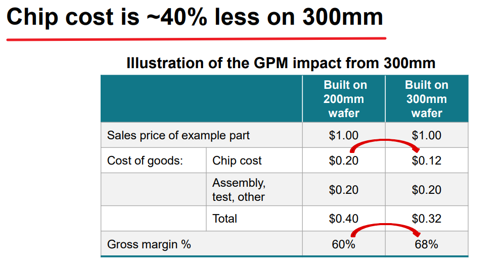
- Cost reduction leads to potential output value growth: The production of 300mm wafers has provided Texas Instruments with significant cost advantages. The combination of internal 300mm wafer production and manufacturing effectively reduces costs. Compared to 200mm wafer manufacturing of unpackaged chips, costs are reduced by approximately 40%. This cost advantage allows the company to be more competitive in product pricing, enabling higher profits at the same price or expanding market share by lowering prices, thereby driving output value growth. As the proportion of 300mm wafer production continues to increase, the cost advantage will further amplify, creating more potential output value for the company.
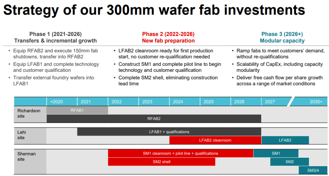
- Capacity expansion supports output value growth: The company is actively investing in 300mm wafer capacity construction, currently making related investments in three factories in Richardson, Lehi, and Sherman. In 2024, the company is expected to make significant progress in 300mm wafer manufacturing, such as RFAB2 continuously increasing output, and LFAB1 has already achieved product mass production at 65nm and 45nm. In the future, by 2030, it is expected that over 95% of wafers will be produced internally, with 300mm wafers accounting for over 80%. The continuous expansion of capacity enables the company to meet market demand for products, directly driving output value growth. As capacity is gradually released, the company’s revenue is expected to further increase, providing strong support for output value growth.
- Optimized product cost structure: The application of 300mm wafers has optimized the cost structure of Texas Instruments’ products. Taking embedded business as an example, products that were originally outsourced have been shifted to internal 300mm network production, resulting in significant cost advantages from a cash perspective. For instance, a wafer that originally cost about $2500 now has a substrate cost of only a few hundred dollars when produced internally. This substantial cost reduction makes the products more price-competitive in the market, helping to increase market share.
- Meeting high-end product demands: 300mm wafer technology helps Texas Instruments meet the manufacturing demands of high-end products. In the automotive and industrial markets, the performance and reliability requirements for semiconductors are continuously increasing. The company utilizes 300mm wafer manufacturing technology to produce products that meet these market demands, such as advanced driver assistance system (ADAS) chips in automotive electronics and high-performance controller chips in industrial automation. These high-end products, with their excellent performance, further enhance the company’s competitiveness in the market.
- Supporting market share expansion: With the cost advantages and enhanced product competitiveness brought by 300mm wafers, Texas Instruments has a stronger position in the market, helping to expand market share. In market competition, the company can attract customers with more competitive prices and higher quality products, thereby gaining more orders and market share in core markets such as industrial and automotive. As market share expands, the company’s business scale will further grow.
- Supporting the development of emerging businesses: 300mm wafer technology supports the development of Texas Instruments’ emerging businesses. In the data center field, the company is increasing R&D investment, utilizing 300mm wafer manufacturing technology to develop products suitable for data centers, such as efficient power management chips and network communication chips. These products meet the data center’s demand for high-performance, low-power semiconductors, driving the company’s development in the data center business field.
- Analog Chips: As a leader in the analog chip field, Texas Instruments leverages 300mm wafer manufacturing technology to mass-produce various analog chips. In power management chips, higher integration is achieved through 300mm wafers, integrating multiple power management functions on a single chip, providing efficient and stable power conversion and management for electronic products, widely used in consumer electronics such as smartphones, tablets, and laptops, as well as industrial equipment and automotive electronics. In signal chain chips, high-performance amplifiers, filters, analog-to-digital converters (ADC), and digital-to-analog converters (DAC) can be manufactured using 300mm wafers. For example, in communication base stations, these signal chain chips can accurately process and convert RF signals, ensuring stable transmission of communication signals.
- Embedded Processors: Texas Instruments uses 300mm wafer technology to develop various embedded processors. In the microcontroller (MCU) product line, 300mm wafers enable chips to integrate more functional modules, such as larger memory capacity and rich communication interfaces (including SPI, I2C, UART, etc.), to meet the needs of different application scenarios. In industrial automation, these high-performance MCUs can be used to control the actions of industrial robots and monitor the operating status of automated production lines; in smart home devices, they can achieve intelligent control and interconnectivity of home appliances. In digital signal processors (DSP), the 300mm wafer manufacturing process enhances the chip’s computing speed and data processing capabilities, suitable for applications with high signal processing requirements, such as audio and video processing, motor control, and radar signal processing. For example, in smart security cameras, DSP chips can perform real-time analysis and processing of captured video images, enabling intelligent functions such as target recognition and behavior analysis.
- RF Chips: In the development of RF chips, 300mm wafer technology plays an important role. Texas Instruments utilizes this technology to manufacture RF chips suitable for wireless communication, such as Bluetooth, Wi-Fi, NFC, and other wireless connection chips. For instance, in Bluetooth chips, the 300mm wafer manufacturing process improves chip integration and performance while reducing power consumption, making them widely used in wearable devices, smart homes, and IoT devices, achieving low-power and stable wireless communication connections between devices. In the 5G communication field, 300mm wafers help produce high-performance RF front-end chips, including power amplifiers, low-noise amplifiers, and RF switches, enhancing the signal transmission and reception capabilities of 5G communication devices, ensuring the efficient operation of 5G networks.
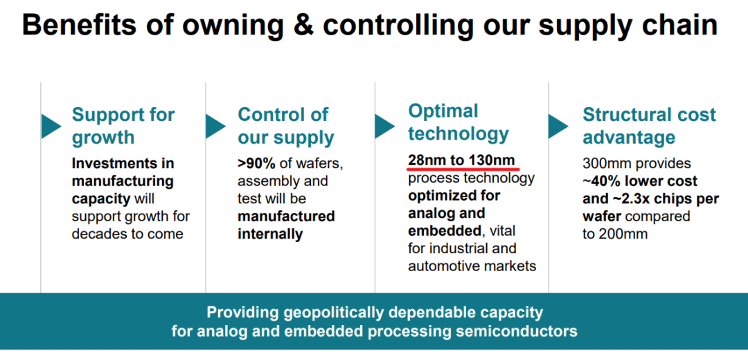
① Opinion: The construction of 300mm will allowover 90% of wafers and assembly to be manufactured internally, with process technology focused on 28nm to 130nm, optimized for analog and embedded products.
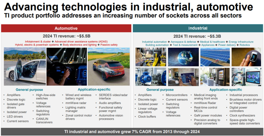
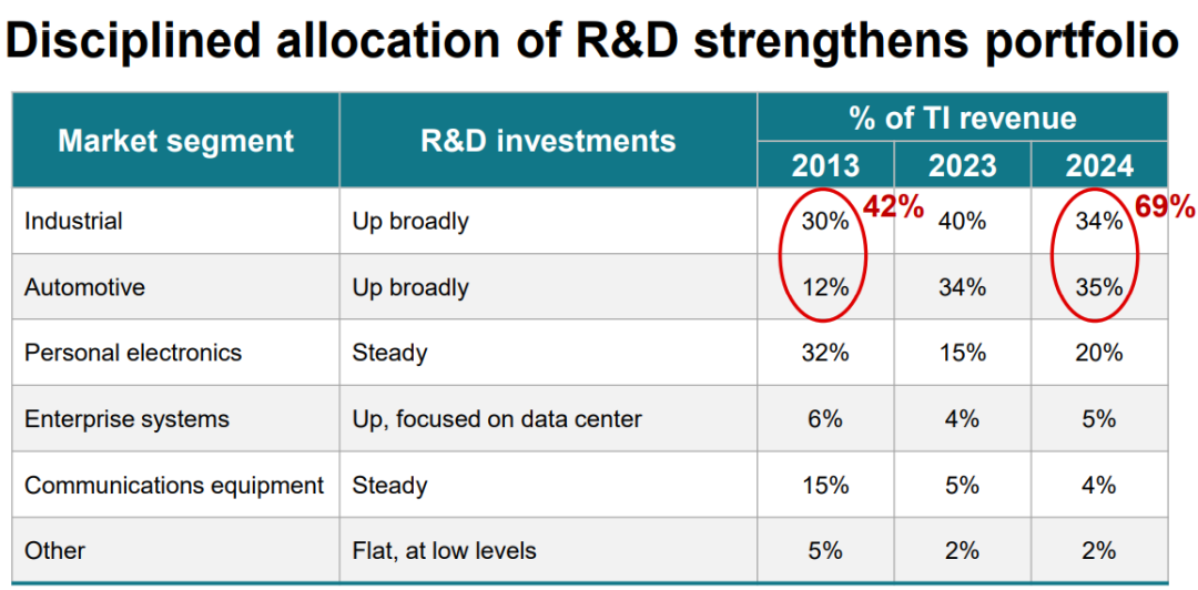
② Opinion:In the industrial and automotive sectors (investing in low-power MCUs, real-time control, wireless connectivity systems, and a very powerful sensor product portfolio including radar), strategic progress has been made, and by 2024, these markets will account for nearly 70% of TI’s revenue, compared to only 42% in 2013.
③ Opinion: 300mm is used for 28nm to 130nm processes, with products involving microcontrollers and analog products (BCD process).
Issue 1: Texas Instruments’ Process Line