
Source: Content from Synopsys Zhihu, thank you!
Chips, as the core components of modern electronic products, have always played the role of the “brain”. Their technological content and capital investment are extremely intensive, with production lines costing tens to hundreds of billions of dollars.The complete process of chip manufacturing includes several main stages: chip design, wafer manufacturing, packaging, and testing, each of which reflects technology and science.For chips, both design and process are equally complex. The birth of EDA technology in the 1980s – automated chip design – greatly reduced the difficulty of chip design and ultra-large-scale integrated circuits. Engineers only need to describe the chip’s functions using a chip design language and input it into a computer. The EDA tool software then compiles the language into a logic circuit, which can then be debugged. Just as editing a document requires Microsoft Office and image editing requires Photoshop, chip developers use EDA software platforms for circuit design, performance analysis, and generating chip circuit layouts. Nowadays, a single chip has billions of transistors; without EDA tools, high-end chip design is simply impossible. Just think about it, how can such a vast project be accomplished manually?The key point is that even with EDA, it does not mean that chip design is easy. Chip design remains a complex system engineering that integrates high precision and cutting-edge technology.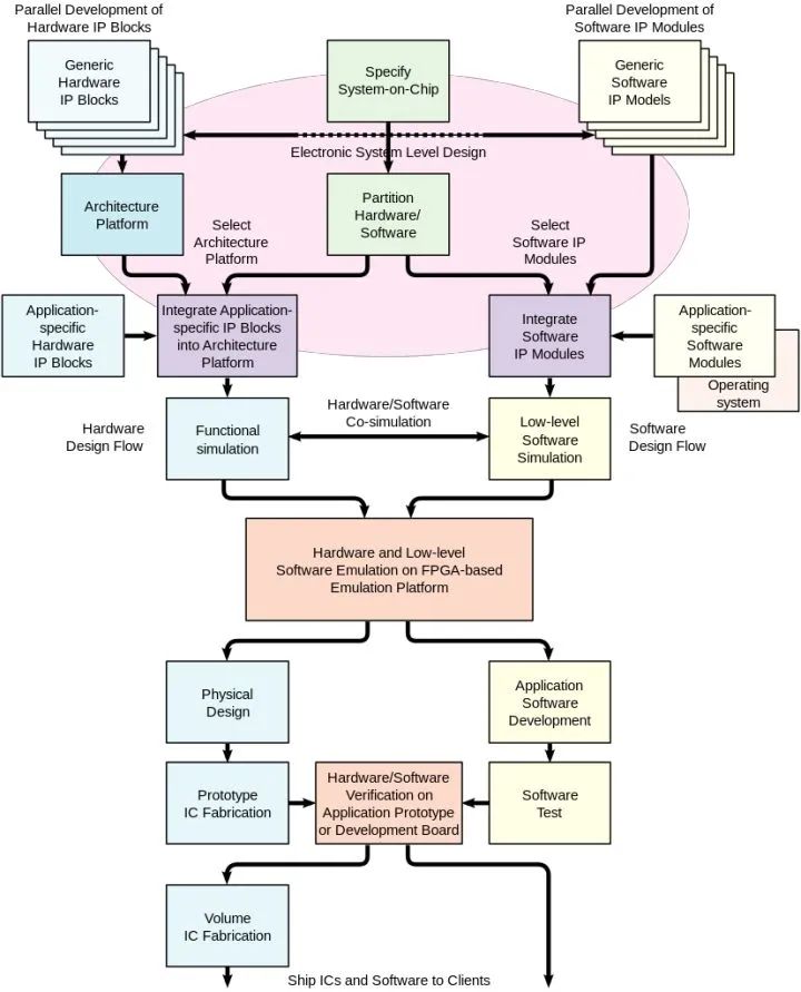 Image from the internet, please delete if infringing.Whether it is IDM or fabless, a common feature is that chip design is at the core of the industry. For example, in 2018, AMD’s processors were manufactured by TSMC using a 7nm process, while Intel’s processors were still using a 14nm process, yet their performance still suppressed AMD, indicating that chip design is also very crucial.To design a chip, developers must first clarify the requirements, determine the chip “specifications”, and define key information such as instruction set, functions, input/output pins, performance, and power consumption. They divide the circuit into multiple small modules and clearly describe the requirements for each module.Then, “front-end” developers design the “circuit” based on the functionality of each module, using computer languages to establish models and verify their functionality accurately. The “back-end” developers then design the “layout” based on the circuit, systematically imprinting billions of circuits onto a silicon chip according to their connection relationships.Only then is the chip design considered complete. Such a complex design cannot have any defects; otherwise, it cannot be repaired and must be started over. If redesigning and processing, it generally takes at least a year and requires an investment of millions of dollars, sometimes even hundreds of millions.Take note, with glasses on, since everyone has a general understanding of the difficulty of chip manufacturing, this article hopes to provide a common understanding of the challenges in chip design.
1
The First Challenge: Difficulty in Architecture Design
Chip design involves many stages, each facing numerous challenges. Taking the relatively simple digital integrated circuit design as an example, the design usually adopts a top-down approach, which includes:Requirement Definition: Analyzing external environments, supply chain resources, and the company’s positioning to propose requirements for the next-generation product. Further considerations include the product’s role, functions, required board quantity, and types of integrated circuits used, precisely defining product requirements. The difficulty in this stage lies in accurately judging future trends in the market and technology, as well as fully understanding the capabilities of designers, manufacturing plants, and the industry chain.Function Implementation: Describing the goals that the chip needs to achieve, usually written in hardware description language. The difficulty here lies in grasping the overall performance and functionality that the chip can achieve, ensuring it meets the goals without exceeding its capabilities.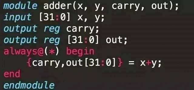 Image source from the internet, please delete if infringing.Structure Design: Dividing the chip into clearly defined sub-modules with clear interfaces and independent functions based on the chip’s characteristics. The difficulty in this stage lies in familiarity with the chip’s structure and whether it can meet requirements with the fewest modules and the lowest standards.Logic Synthesis: Developers convert hardware description language into logic circuit diagrams. The difficulty here is ensuring the code is synthesizable, clear, concise, and readable, while also considering the reusability of modules.
 Image source from the internet, please delete if infringing.Physical Implementation: Converting logic circuits into physically connected circuit diagrams. The difficulty here lies in how to map from RTL descriptions to synthesis library units using as few components and connections as possible, obtaining a gate-level netlist that meets area and timing requirements while ensuring internal interference is minimized.Physical Layout: Handing over the layout in GDSII file format to the wafer factory to create the actual circuit on the silicon chip, followed by packaging and testing to obtain the physical chip.It must be noted that during chip design, many variables need to be considered, such as signal interference and heat distribution. The physical properties of chips, like magnetic fields and signal interference, vary greatly under different processes. There are no mathematical formulas for direct calculation, nor applicable empirical data to directly fill in; it relies solely on EDA tools to design step by step, simulating repeatedly and making trade-offs. After each simulation, if the results are unsatisfactory, redesigning is necessary, which tests the team’s wisdom, energy, and patience significantly.
2
The Second Challenge: Difficulty in Verification
The goal of chip verification is to iteratively validate through checks, simulations, and prototype platforms before chip manufacturing, to discover system software and hardware functional errors in advance, optimizing performance and power consumption, ensuring the design is accurate, reliable, and meets the initial planned chip specifications.It is not a process that occurs after the design is completed but is a repetitive behavior that runs through every stage of the design, which can be subdivided into system-level verification, hardware logic function verification, mixed-signal verification, software function verification, physical layer verification, timing verification, etc.Verification is challenging; first, verification can only disprove, requiring repeated consideration of potential issues and using formal verification methods to ensure correctness probability, which greatly tests the experience and wisdom of designers.Secondly, the methods of verification must be as efficient as possible. Modern chips integrate microprocessors, analog IP cores, digital IP cores, and memory (or external memory control interfaces), leading to exponential growth in verification complexity. How to quickly, accurately, completely, and easily debug increasingly complex verifications to enter the tape-out stage is the biggest challenge for every chip designer.Finally, there are challenges with the verification tools themselves. Taking common FPGA hardware simulation verification as an example, in the 90s, FPGA verification supported a maximum of 2 million gates, with each gate costing 1 dollar. Although the unit price has significantly decreased now, with the exponential increase in chip complexity, the number of gates in verification has risen to tens of millions and billions, making the overall costs even more staggering.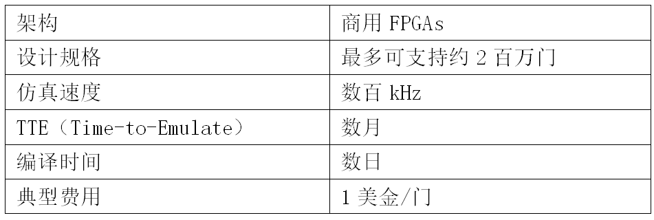 Image source from the internet, please delete if infringing.Additionally, FPGA itself is also a type of chip design. Now large designs (greater than 20 million equivalent ASIC gates) require multiple FPGA interconnections for verification. The design of FPGA faces practical requirements such as splitting RTL logic, interconnection topologies between multiple FPGAs, I/O allocation, layout, and observability, adding further complexity to the design stage.
3
The Third Challenge: Difficulty in Tape-Out
Tape-out refers to trial production. After design completion, the chip foundry produces a small batch for testing. It appears to be chip manufacturing but actually belongs to the chip design industry.Tape-out is not technically difficult because chip design is based on existing processes. Aside from a few productions requiring guidance from chip design companies, the difficulty lies in money, money, money.How expensive is tape-out? Let’s reference the public quotes from CMP (Circuits Multi-Projets, a non-profit multi-project wafer service organization in the U.S.).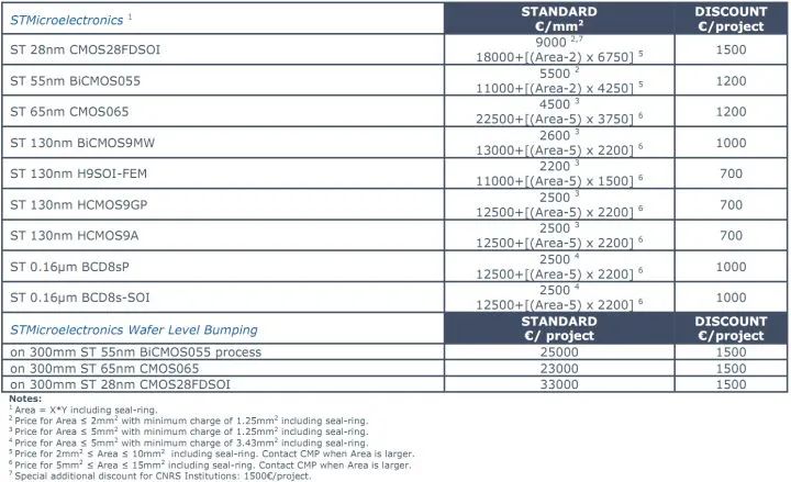 Image from CMP price list.According to this quote, taking the smallest die area processor, Qualcomm Snapdragon 855 (dimension 8.48 mm × 8.64 mm, area 73.27 square mm), the standard price for tape-out using a 28nm process is €499,072.5, which is nearly 4 million RMB!Then, what can the chip design company obtain? 25 bare chips, averaging 160,000 RMB each!More importantly, tape-out is not a one-time thing!If tape-out fails, modifications are needed for a second tape-out; if tape-out succeeds, further modifications and optimizations may require a second tape-out.Each time requires at least several hundred thousand RMB.What does it mean to spend money? This is what it means!Some may question why this cost issue is considered a difficulty. This is certainly a difficulty; isn’t the biggest difficulty in the world the lack of money?The reason for mentioning tape-out costs is that many people point out that establishing an advanced process chip production line requires massive capital investment, but tape-out shows that chip design also has an astonishing thirst for funds.
4
The Fourth Challenge: Increasingly Challenging Design Requirements
First, as chip usage scenarios extend to AI, cloud computing, smart vehicles, 5G, etc., the safety and reliability of chips have become unprecedentedly important, imposing higher and stricter requirements on chip design.Secondly, with the rapid development of AI and smart vehicles, new architecture requirements for dedicated chips and industry-adaptive designs arise, presenting more new challenges to chip design.Finally, as silicon-based chips approach the 1nm process limit according to Moore’s Law in the next two to three years, the responsibility for continuing to improve performance and reduce power consumption increasingly falls on chip design, putting greater pressure on chip designers. Additionally, advancements in process technology urgently require guidance from chip design to realize, further increasing the pressure.
Disclaimer: The content of the article represents the author’s personal views. Chip Driver reposts it only to convey a different perspective and does not imply Chip Driver’s endorsement or support of this view. If there are any objections, please contact us.
Recommended Reading
1. The Semiconductor Talent Market’s “Reverse Flow” After the Frenzy of High Salaries!2. IC Employment “Recommendation” Bonuses: Recommend Students to Win Cash Prizes!3. Distribution of Chip Companies in Xi’an! “Western Silicon Valley” Has Great Potential!4. Introduction to the Graduate School Situation of Nine Model Microelectronics Institutions! It Turns Out That Choosing a School Reasonably Can Lead to Success!5. What Are the Differences Between ASIC and FPGA Design, and Which Has a Better Development Prospect?……

E Course Network (www.eecourse.com) is a professional integrated circuit education platform under Moore Elite, dedicated to cultivating high-quality integrated circuit professionals in the semiconductor industry. The platform is oriented towards the job demands of integrated circuit companies, providing a training platform that fits the corporate environment, and rapidly cultivating students to meet enterprise needs through online and offline training methods.
E Course Network was established in 2015, with a mature training platform, a complete course system, and strong teaching resources, planning a high-quality course system of 168 courses covering the entire integrated circuit industry chain, and has 7 offline training bases. E Course Network has a total of 517,000 fans online and has directly supplied 8,127 professional talents to the industry. It has established deep cooperative relationships with 85 universities and held 240 corporate IC training sessions.