
Source: Chip Learning
Original Author: Chip Future
The semiconductor wafer fabrication NRE refers to “Non-Recurring Engineering” costs, which are one-time expenses incurred during the chip development process. These costs cover a series of non-recurring work from chip design to the successful first wafer fabrication, including design and R&D expenses, mask production costs, process development and optimization costs, testing plan formulation, and preparation of testing equipment.In MEMS, NRE is generally proposed by the foundry and is approximately equivalent to the concept of “process development,” referring to the first successful process run of MEMS at foundry A, without considering yield improvement for the wafer fabrication. If NRE has already been completed at foundry A and is successful, switching to foundry B will still require undergoing B’s NRE.In MEMS, there is a fascinating phenomenon where after completing NRE for a product, customers receive 12-25 wafers, which is sufficient for several years, with no subsequent mass production. Due to the small volume characteristic of MEMS, many foundries charge a significant NRE fee, but some MEMS foundries are willing to refund or discount NRE fees based on a certain number of wafers during the mass production phase.The costs during the NRE stage at foundries vary based on different products, generally ranging from 300,000 to 1,000,000 RMB. The basic NRE quotation from foundries is determined by the number of photolithography steps, whether there are furnace tube processes, whether there are sacrificial layer processes, and whether precious metals are involved. Additionally, new MEMS foundries may also include equipment depreciation costs.MPW (Multi Project Wafer) generally refers to placing multiple integrated circuit designs that use the same process on the same wafer, as opposed to a full mask. This allows a single manufacturing process to handle multiple IC design tasks. It is suitable for chip designs that are still in the R&D phase, uncertain market response, or do not require large-scale mass production. For example, universities, research institutions, and independent designers often use MPW for chip design verification, as well as small and medium design companies developing new products.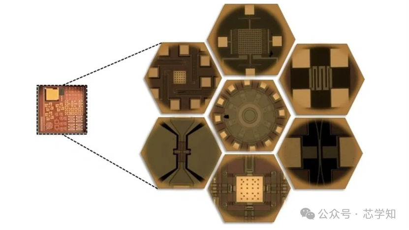 Figure: MPW within a single SHOT
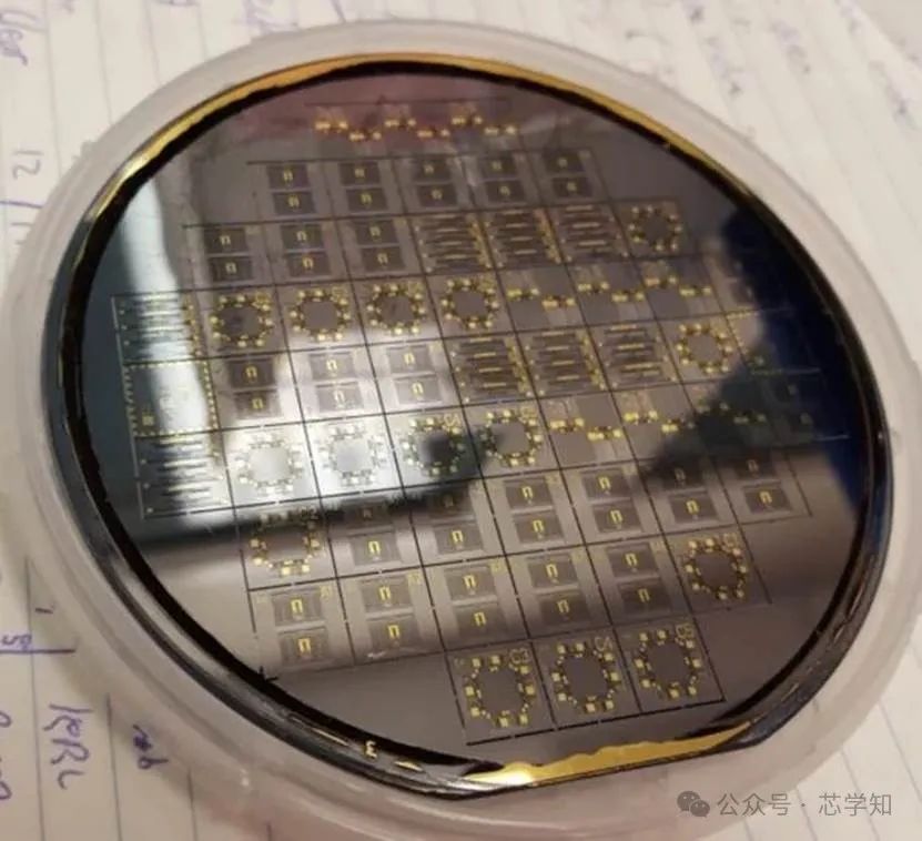 Figure: MPW on a waferIt is relatively difficult to conduct MPW in MEMS, especially during the mass production phase where MPW wafers do not appear. MEMS design and processes are more complex than ICs, involving multiple physical fields in design and body silicon or sacrificial layer processes in manufacturing. It is challenging to place different products on the same wafer, and even difficult to place different specifications of the same series of products on one wafer. For example, in pressure sensors, different ranges have different membrane thicknesses, making it impossible to fabricate dies with varying membrane thicknesses on the same wafer. Therefore, in MEMS wafer fabrication, MPW often appears during the NRE stage to validate the advantages and disadvantages of different MEMS designs and provide optimization directions for the next round of design.
END
Reprinted content only represents the author’s views
It does not represent the position of the Semiconductor Institute of the Chinese Academy of Sciences
Editor: Yi Er
Reviewer: Mu Xin
Submission Email: [email protected]
Previous Recommendations
1. The Impact of Crystal Growth Process on the Oxygen Content of N-type Monocrystalline Silicon
2. Titanium Nitride (TiN) in Chip Manufacturing
3. Differences Between Microwave and Low-Frequency Radio Waves/High-Frequency Optical Waves
4. Understanding the Principles and Classifications of Photodetectors
5. Four Futures of Deep Space Chips