Motivation:The short-circuit protection methods for power devices can be divided into two main categories: detecting short-circuit current and detecting voltage drop. The current detection method is commonly done through a Sense FET or a shunt resistor, while voltage detection is referred to as desaturation protection. Most power modules do not have an integrated Sense FET, and adding an external shunt resistor increases system costs, making desaturation protection a more common short-circuit protection method in the industry.For example, in the case of an IGBT, under normal operating conditions, the IGBT operates in the saturation region when conducting and in the cutoff region when turned off, needing to traverse the amplification region during the turn-on and turn-off processes. When a short circuit occurs in the IGBT, its operating point shifts from the saturation region to the amplification region, which is the high voltage and high current area, referred to as desaturation. By monitoring the collector-emitter voltage (VCE) of the IGBT, a short circuit can be identified.Realization:Diode-type DESAT Circuit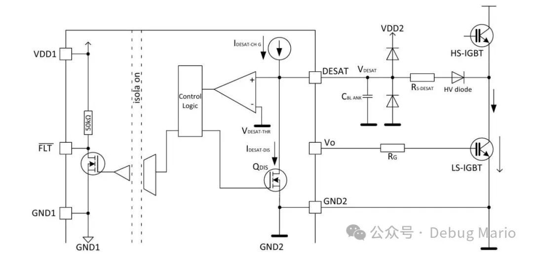 For MOSFETs or IGBTs, during the off state, they typically withstand high voltage across their terminals, making it impossible to directly sample the voltage across the power device. Therefore, a high-voltage diode is first placed between the drain and the DESAT pin.
-
When the input to the driver chip is floating or at a low level, the DESAT pin is pulled low by an internal MOSFET (Q_DIS) to avoid false triggering, while discharging C_BLANK.
-
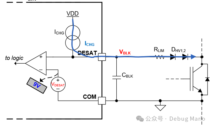
When the input signal level is high, as shown in the following IGBT example, the voltage across VCE may be 2V during normal conduction. The internal pull-up current source I_CHG flows out from the DESAT pin through R_LIM and D_HV to the IGBT. At this point, the voltage drop across C_BLK, which is the voltage across the DESAT pin, is approximately the IGBT_VCE drop plus the forward conduction voltage drop of the high-voltage diode plus the voltage drop across R_LIM. At this moment, V_DESAT no longer increases and remains below the DESAT protection threshold.
-
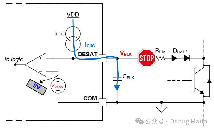
When the input signal level is high and a short circuit occurs, as shown in the following diagram, the voltage drop across VCE will rise rapidly. At this point, the high-voltage diode will become reverse-biased, and the internal current source will only have one direction of flow, which is to charge the capacitor C_BLK. When the voltage drop across C_BLK, which is the DESAT voltage, exceeds the threshold voltage, short-circuit protection will be triggered.
The specific working principle is illustrated in the following diagram.
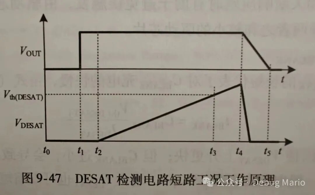
(1) t0~t1: The input to the driver chip is low, and the output Vout is also low. The switch is in the off state, so the high-voltage diode is reverse-biased. T_DESAT is in the conducting state, discharging C_BLANK, making the voltage across it 0V, and I_DESAT also flows to GND through T_DESAT.
(2) t1~t2: T_DESAT transitions to the off state.
(3) t2~t3: The output Vout of the driver chip is high, but due to the short circuit in the power device, I_DS rises rapidly, and V_DS remains at a high voltage, while the high-voltage diode remains reverse-biased. I_DESAT continuously charges C_BLANK, and V_DESAT begins to rise linearly from 0V.
(4) At time t3: V_DESAT rises to V_DESAT(th), triggering the protection comparator.
(5) t4~t5: T_DESAT transitions to the conducting state, discharging C_BLANK, and the driver chip turns off the power device.
Based on the above analysis, DESAT protection can be divided into four stages: DESAT delay (t1~t2), blanking time t_BLANK (t2~t3), turn-off response delay (t3~t4), and device turn-off (t4~t5). To quickly complete short-circuit detection and turn-off, it is necessary to minimize the total duration of these four stages.
Conclusion:
1. The DESAT delay and turn-off response delay help avoid false triggering, determined by the driver chip, and cannot be avoided. Therefore, it is necessary to choose a driver chip with a smaller sum of both.
2. The duration of the blanking time t_BLANK represents the speed of charging C_BLANK, given by the following formula:
t_BLANK = C_BLANK*V_DESAT(th)/I_DESAT
It can be seen that reducing C_BLANK can make V_DESAT rise faster, but if C_BLANK is too small, it may lead to interference and false triggering. C_BLANK is generally chosen to be between 100~330pF. Increasing I_DESAT can also shorten the blanking time, so a driver chip with a relatively large I_DESAT can be selected. The driver chip’s I_DESAT is generally around 500μA. When V_DESAT(th) is 9V and C_BLANK is 100pF, the calculated t_BLANK is 1800ns. To further shorten t_BLANK, C_BLANK can be connected to the power supply of the driver chip through a pull-up resistor (though this will increase the power consumption of the driver chip) or to the output V_OUT (noting the negative voltage withstand capability of the DESAT pin during negative voltage turn-off) to increase the charging current.
3. To avoid false triggering from interference sources in the system, a deglitch filter digital filter can also be designed internally for DESAT at the software design level. Only when the DESAT voltage exceeds the threshold for a time longer than this filter window will the desaturation protection be triggered. In TI’s SPI-type drivers, this parameter is configurable in multiple stages. Using a longer window time can effectively avoid false triggering from system interference, but it will also increase the short-circuit detection time and energy. From the hardware design perspective, it is essential to minimize the junction capacitance of the high-voltage diode. Since the DESAT circuit samples the voltage at the drain-source level of the power device, the dv/dt generated during the switching process will charge and discharge C_BLANK through the junction capacitance of the high-voltage diode. Positive dv/dt will supply current to DESAT, while negative dv/dt will pull current from DESAT. Therefore, careful attention must be paid to the junction capacitance parameters when selecting high-voltage diodes, and if necessary, two high-voltage diodes can be connected in series to reduce the equivalent parasitic capacitance.
4. There are two scenarios for turning off the device: hard turn-off and soft turn-off. Hard turn-off is performed directly through the normal turn-off circuit, resulting in a shorter turn-off time. To prevent the turn-off voltage spike V_DS(spike) from exceeding the device’s voltage rating during turn-off under high current, after triggering the DESAT short-circuit protection, the driver chip performs a slow turn-off of the device through a high-impedance drive circuit, known as soft turn-off.
Reference:
[1] Texas Instruments Application Guide for Desaturation Protection (DESAT):
https://zhuanlan.zhihu.com/p/698138611https://www.ti.com.cn/cn/lit/an/zhcadl7/zhcadl7.pdf
[2] Silicon Carbide Power Devices: Characteristics, Testing, and Application Technologies