Editors: Zhang Qian, Dan Jiang
Although it’s a 130nm process, it’s ultimately free, and there’s a tutorial that teaches you step by step. What more could you want?
Yesterday, Google’s open-source blog [1] announced that the company’s hardware toolchain team is launching a new developer portal to help small developer communities start their own Open MPW shuttle projects. Google will assist small open-source chip projects in chip manufacturing, and it will be free.
MPW stands for Multi Project Wafer, which involves placing multiple integrated circuit designs that use the same process on the same wafer for fabrication. After manufacturing is completed, each design can obtain dozens of chip samples, which is sufficient for experimentation and testing during the prototype design phase. MPW is somewhat similar to group buying, where the wafer foundry provides a specific time for chip companies to tape out together, a process also known as Shuttle.[2]
Generally, the cost of each Shuttle is shared by all companies participating in the MPW project based on die size. However, in Google’s Open MPW shuttle project, these costs have been waived.
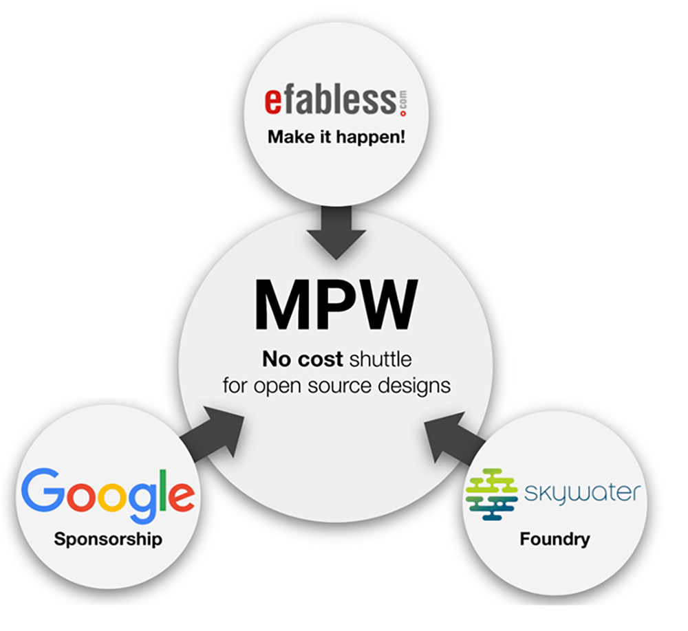
The Open MPW shuttle project began in November 2020 on the chip design service platform Efabless, with fabrication completed on the open-source SkyWater 130nm process. The project is open to everyone as long as your project is completely open-source and meets some other requirements. Google covers the costs of manufacturing, packaging, evaluation PCB boards, and shipping.
Project homepage: https://platform.efabless.com/open_shuttle_program
This initiative has garnered a lot of developer support: MPW-1 received 45 design submissions within a month, MPW-2 received 56 submissions in 30 days. The MPW-5 activity, which ended in March this year, received 78 chip project submissions from 19 countries, achieving record participation levels.
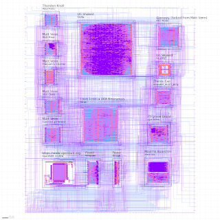
Each project has a fixed user area of 2.92mm x 3.52mm and 38 I/O pins, and provides the necessary testing infrastructure to verify chip specifications and performance before submission.
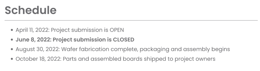
The submission deadline for the next MPW-6 open project is set for June 8, 2022. Projects submitted for MPW-6 will complete wafer fabrication by the end of August, with packaging and assembly starting thereafter. By mid-October, project submitters will receive their designed chip parts and assembly boards.
To help everyone design their chips more smoothly, Google has launched a new developer website that includes various introductory tutorials and operational guides:
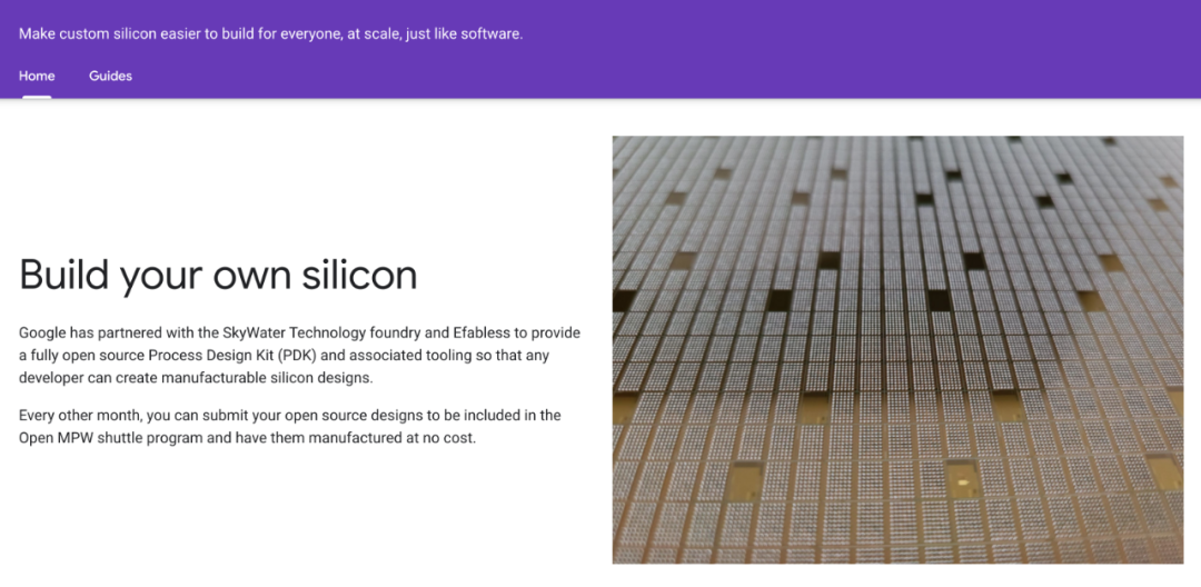
Website address: https://developers.google.com/silicon
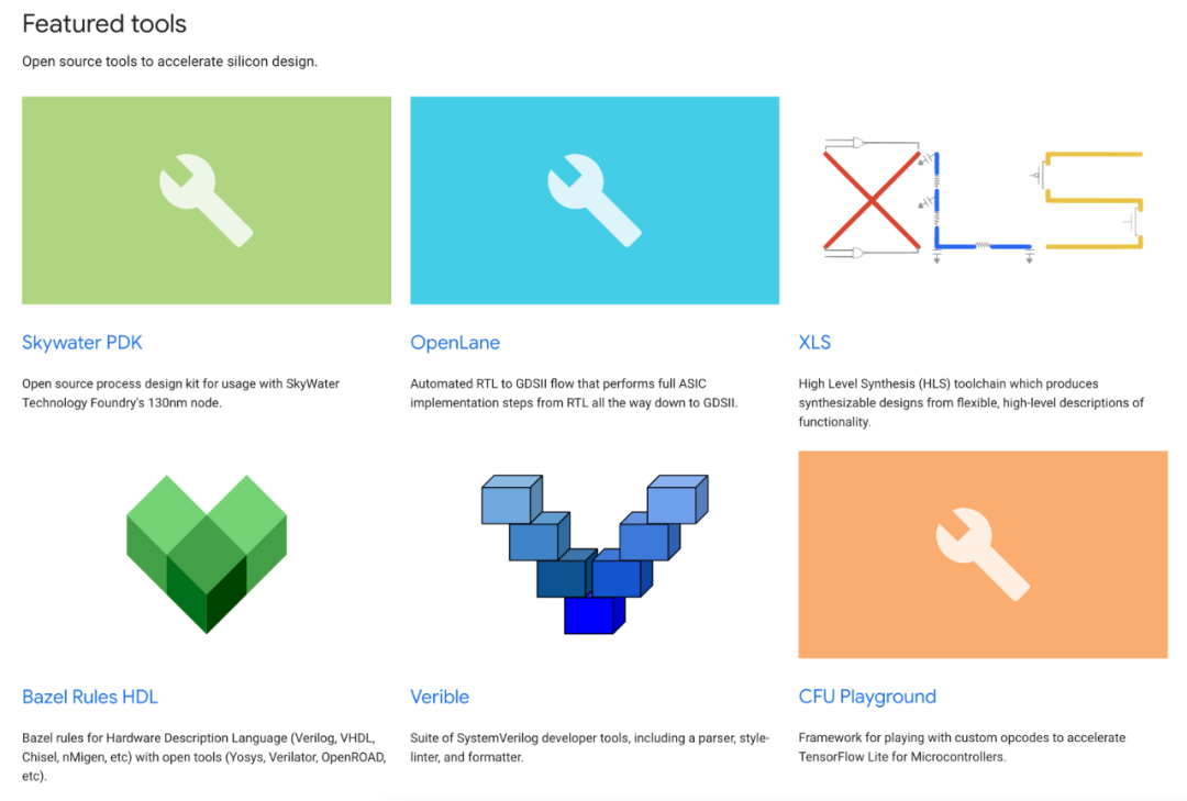
This site provides sections such as “Get started” and “Featured tools.”
The “Get started” section includes a multi-stage learning path from beginner to advanced.
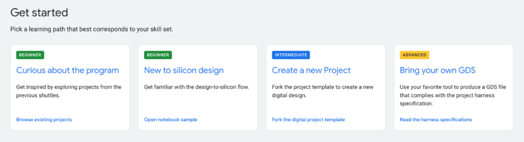
In the beginner phase, the “Curious about the program” module contains all past MPW project submissions for reference by developers who wish to participate; “New to silicon design” provides code examples of the chip design process.
After getting started, developers can refer to the “Create a new Project” section to continue their design; this guide includes all the work that needs to be done before submission; additionally, “Bring your own GDS” provides methods for creating GDS files.
Moreover, this website also introduces several featured open-source tools that help accelerate chip design:
Why did Google launch such a project?
Google explained in the blog that the launch of the Open MPW shuttle project is based on two considerations: first, Moore’s Law is nearing its end, and the traditional approach of cramming more transistors onto limited silicon wafers is no longer sustainable. Therefore, we need to develop more efficient dedicated hardware accelerators; second, with the trend of the Internet of Things (IoT), the number of IoT devices is growing exponentially, but the current global chip supply chain is facing difficulties, with delivery times for popular ICs sometimes exceeding a year. Thus, it is essential to fully tap into the existing capacities of global chip foundries and leverage their mature node processes to address the supply shortage.
Mature process nodes like SKY130 (a 130nm technology) provide a great way for IoT application prototypes, which typically need to balance cost, power consumption, and performance, while utilizing a mix of analog blocks and digital logic in the design. They offer faster turnaround times than cutting-edge process nodes, while the cost is just a fraction, significantly reducing the trial-and-error and iteration time in chip design.
What projects have participated in past shuttles?
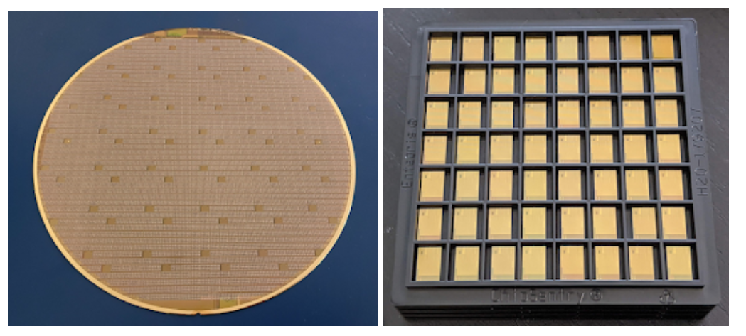
So far, Google has assisted around 250 open-source projects in completing shuttles.
-
Small digital, analog, and mixed-signal designs;
-
Analog, SRAM, ReRAM generators;
-
Dedicated encryption, ML computation accelerators;
-
Some interesting designs, such as Sudoku accelerators, guitar string physical modeling, hardware versions of Tetris or Wordle crossword games, etc.;
-
Many system-on-chip designs, ranging from award-winning RISC-V cores to larger Linux-capable 64-bit SoCs.
What requirements must projects meet to participate in shuttles?
Open-source projects participating in the shuttle must meet the following requirements:
-
The project must target the currently supported 130nm process SkyWater Open PDK.
-
The project must be published on a git-compatible repo and be publicly accessible.
-
The top-level of the project must include an approved open-source license file, must indicate third-party source code, and the source code must include correct titles.
-
The repo must contain project documentation and comply with Google’s inclusive language guidelines.
-
The project must be fully open. It must include a GDSII design, and it must be reproducible from the source code included in the project.
-
The project must use the general testing tools and padframe based on the Caravel repo. New projects should start by cloning or forking the Caravel User Project repo and implementing their project using the user_project_wrapper. The Caravel repo is configured as a submodule in the “caravel” directory of the project. Note that it is not necessary to initialize or clone the Caravel subdirectory to complete or submit the project. For more instructions, refer to the project README.
-
The project must successfully pass the Open MPW pre-check tool, including using the reference version of LVS and DRC clean with the OpenLane process. The project should implement and pass simulation test benches to integrate its design into Caravel. The Caravel User Project provides examples of how to achieve this.
[1]https://opensource.googleblog.com/
[2] https://www.jianshu.com/p/face2258013d

© THE END
For reprints, please contact this public account for authorization
Submissions or inquiries: [email protected]