
Source: LightSense Technology
Original Author: LIG
The Waveguide Embedded System (WES) is designed for AI/HPC data centers and can overcome the challenges of CPO integration. WES enables high-density, low-loss, fiber-free optical interconnects from device to device through an integrated optical engine and precise coupling structures.
WES consists of three key components, as shown in Figure 1: optical PCB, optical engine, and coupling structure. The WES channel converts to the optical domain and back, allowing high-speed electrical signals to be transmitted from point (A) to point (B). The optical channel provides seamless data transmission through a highly integrated optical engine in the form of semiconductor packaging and PCB embedded waveguides.
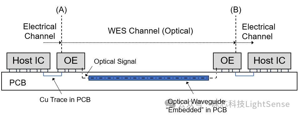
Figure 1. System diagram of the Waveguide Embedded System (WES). The WES channel can provide high-performance optical links from point (A) to (B) within the PCB.
A. Optical Engine
The terminal of the WES channel includes an Optical Engine (OE) that converts electrical data to optical data and vice versa. The OE consists of a VCSEL and driver IC on the Tx side and a PD and TIA on the Rx side, connected by a short-length multimode waveguide.
To achieve seamless integration within the PCB ecosystem, the OE must have dimensions similar to those of other electrical components. Fan-out Wafer-Level Packaging (FOWLP) is an advanced semiconductor packaging method and is one of the most promising technologies for integrating VCSELs and PDs with electronic ICs. LIPAC first introduced Optical System-in-Package (O-SiP) technology and provided the optical engine for this project.
Figure 2 shows the OE based on FOWLP, which is a standard BGA package but without the substrate. The OE is both thin and small, potentially suitable for future increases in physical channel density. The optical window is placed on the BGA side of the package, facing down during assembly, while the top side of the package can be used for heat dissipation.
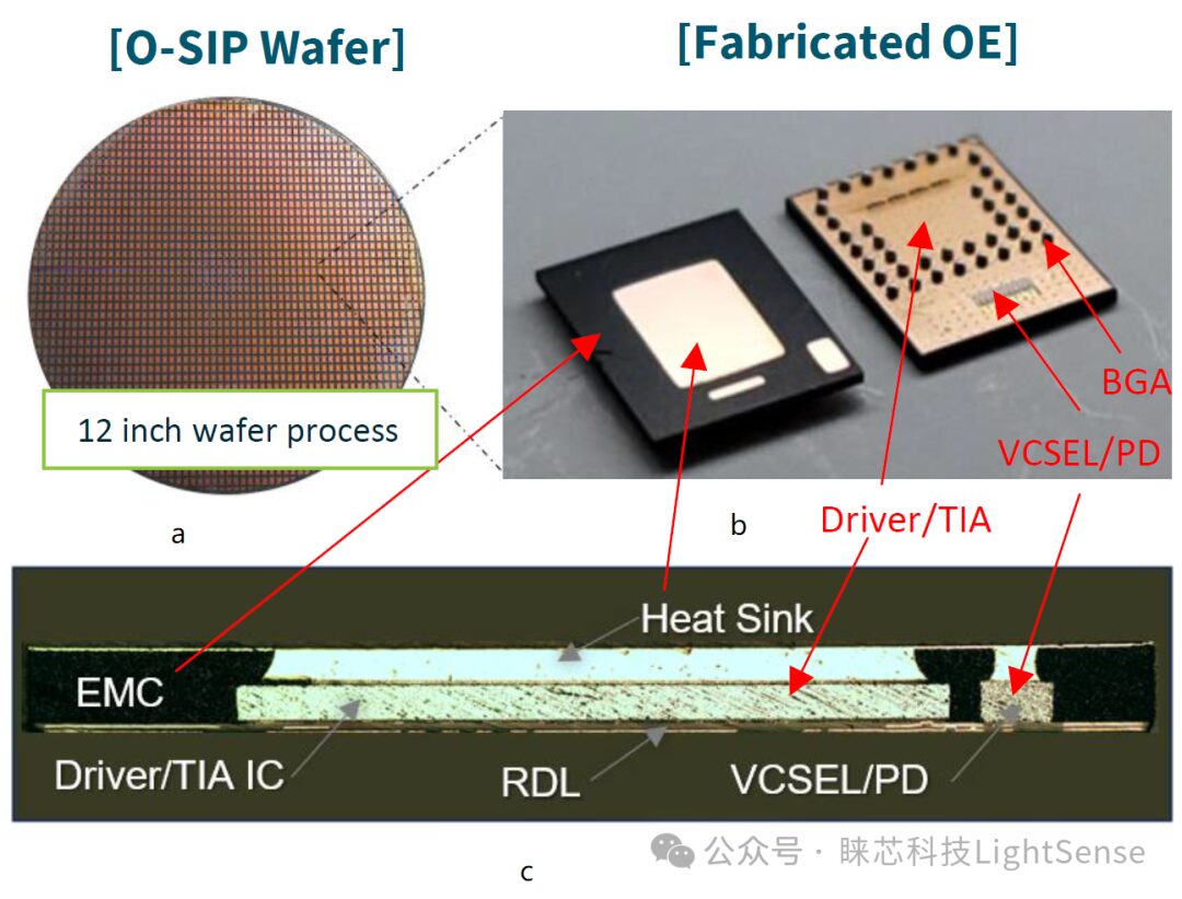
Figure 2. Optical engine manufactured using the FOWLP method. (a) It can be produced in a 12-inch wafer size format. (b) Front and back sides of the WES optical engine. The ball grid array and VCSEL/PD openings can be seen on the back of the OE. (c) Cross-section of the OE. The IC is co-packaged with the VCSEL/PD within EMC materials. Fine electrical layers are formed as RDL in the OE.
B. Optical PCB
The WES includes multimode waveguides embedded in the PCB as optical data transmission channels. Similar to copper traces in PCBs, the optical waveguide layer can be arranged as interconnect traces and can be made from polymer-based materials. The core of the waveguide can be created through contact mask lithography or laser direct imaging (LDI), both of which are compatible with traditional PCB manufacturing processes. A cladding layer of 10-40μm is used to hold a core layer of 40-50μm, as shown in Figure 3 (a).
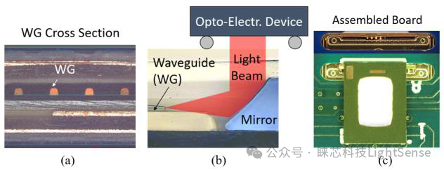
Figure 3. (a) Cross-section of the O-PCB with waveguides (WG). (b) Optical coupling structure between the OE and WG in the O-PCB. (c) Image of the assembled board with OE and coupling mirrors on the O-PCB.
The minimum bending radius is typically about 15mm, while the standard waveguide spacing is approximately 250μm. This allows for higher density, lower loss, and lower crosstalk optical channels compared to electrical channels.
C. Coupling Structure
Concave mirrors are used for optical coupling from the embedded VCSEL in the OE to the waveguide on the Tx side and from the waveguide to the embedded PD in the OE on the Rx side. As shown in Figure 3 (b), the beam is focused into the waveguide and PD. The alignment tolerance of the coupler in the X-Y direction is about ±15μm, and ±40μm in the Z direction. The mirror assembly has guiding structures that fit with benchmarks in the waveguide layer, allowing the mirrors to be assembled onto the PCB and aligned precisely with the waveguides. Figure 3 (c) shows the assembled mirror assembly mounted on the PCB, which features an integrated waveguide structure made from various optical components. Other forms of couplers are also possible. For example, microGlass proposes a dual-chip coupling structure (one for the OE side and another for the PCB side) to improve alignment accuracy.
Demonstrator Assembly
Assembling the OE on the PCB requires higher precision than assembling electrical components. The alignment tolerance is determined by the optical design of the coupling structure. Therefore, careful selection of assembly methods is essential. In the PoC demonstrator, a flip-chip bonder was used to place the OE on the PCB with an alignment tolerance of ±5μm. To use traditional IR reflow methods, epoxy resin was applied between the PCB and the OE before placing the OE. The epoxy resin fixed the position accuracy provided by the flip-chip bonder and prevented movement of the OE during the infrared reflow process.
Figure 4 shows the design and assembly of the OE and OPCB in the PCIe demonstrator. It includes operational circuits for the OE and high-speed coaxial cable connectors to test RF performance. We verified that the VCSEL can be powered in this system. The combined waveguide loss and coupling loss is approximately -6.5dB (in the best case).
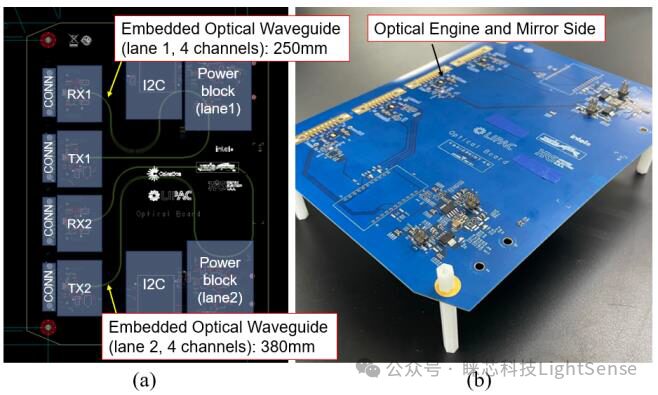
Figure 4. (a) PCB design of the demonstrator, including power blocks, I2C circuits, and RF connectors. (b) All electrical and optical components are manufactured using O-PCB.
END
This content represents the author’s views only.
It does not represent the position of the Institute of Semiconductors, Chinese Academy of Sciences.
Editor: Schrödinger’s Cat
Responsible Editor: Six Dollar Fish
Submission Email: [email protected]