Using Logic Analyzer to View Software Simulated I2C Timing

Using Logic Analyzer to View Software Simulated I2C Timing

Using Logic Analyzer to View Software Simulated I2C Timing

Click here to download the materials (3rd update)

Using Logic Analyzer to View Software Simulated I2C Timing

We are giving away materials, copy and reply with the following keyword to receive them

Material Collection

Using Logic Analyzer to View Software Simulated I2C Timing

Using Logic Analyzer to View Software Simulated I2C Timing

Using Logic Analyzer to View Software Simulated I2C Timing

About Today’s Post

IIC stands for Inter-Integrated Circuit, a simple, bidirectional, two-wire, synchronous serial bus designed by Philips Semiconductor in the early 1980s.
Microcontrollers generally have hardware I2C, so why use software I2C?
Firstly, hardware I2C is difficult to use, unstable, and prone to freezing, especially in multi-slave situations; secondly, I2C is a patented bus, and if the MCU manufacturer provides complete IIC support, they must pay a substantial patent fee to Philips. Many MCU manufacturers like ATMEL avoid this fee by calling I2C TWI, while ST provides a limited I2C functionality.
Of course, there may be more complex reasons, and we still use software to simulate I2C for easier debugging and portability;
The I2C protocol defines the start and stop signals for communication, data validity, acknowledgment, arbitration, clock synchronization, and address broadcasting;

Using Logic Analyzer to View Software Simulated I2C Timing

Using Logic Analyzer to View Software Simulated I2C Timing

Using Logic Analyzer to View Software Simulated I2C Timing

Next, we will simulate I2C using software and view the timing with a logic analyzer:
1. GPIO configuration initializes SCL and SDA to high level;
2. Start signal for communication:
When the SCL line is high, the SDA line transitions from high to low, indicating the start of communication;

Using Logic Analyzer to View Software Simulated I2C Timing

3. Stop signal for communication:
When SCL is high, the SDA line transitions from low to high, indicating the end of communication. Start and stop signals are generally generated by the master.

Using Logic Analyzer to View Software Simulated I2C Timing

4. Data validity
I2C uses the SDA signal line to transmit data and the SCL signal line for data synchronization.
The SDA data line transmits one bit of data for each clock cycle of SCL.
During transmission:
When SCL is high, the data represented by SDA is valid; that is, if SDA is high, it represents data “1”, and if it is low, it represents data “0”;
When SCL is low, the data on SDA is invalid, and at this time SDA transitions to prepare for the next data representation;

Using Logic Analyzer to View Software Simulated I2C Timing

Using Logic Analyzer to View Software Simulated I2C Timing

5. Address and data direction

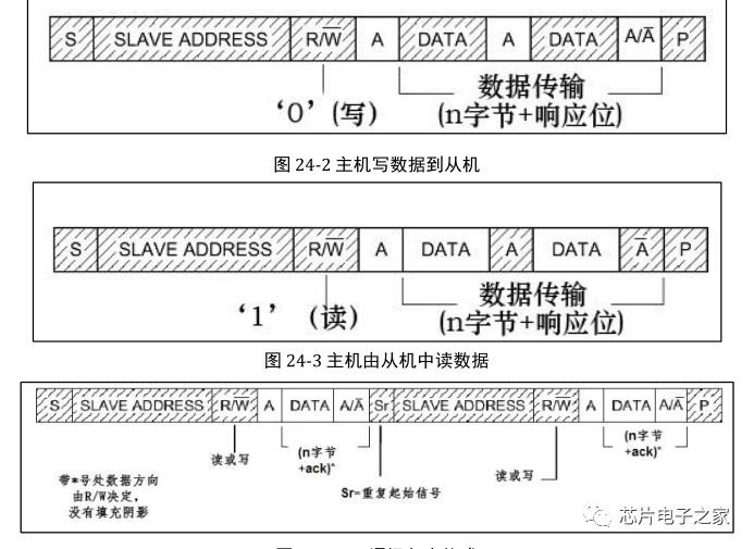
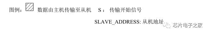
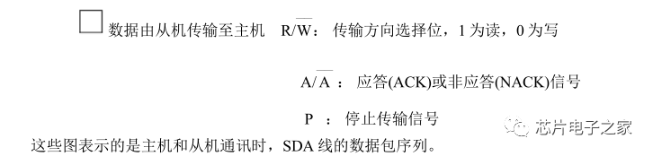
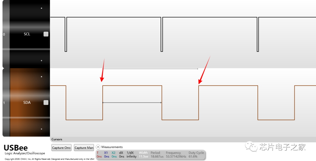
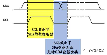
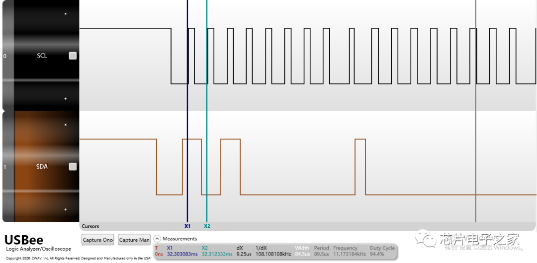
Each device on the I2C bus has its own unique address. When the master initiates communication, it sends the device address (SLAVE_ADDRESS) via the SDA signal line to locate the slave.

In read data direction, the master releases control of the SDA signal line to the slave, which controls the SDA signal line while the master receives the signal. In write data direction, the SDA is controlled by the master while the slave receives the signal.
6. Acknowledgment
Data and address transmissions in I2C include acknowledgment. Acknowledgment consists of two signals: “acknowledge (ACK)” and “not acknowledge (NACK)”. As the data receiver, when a device (either master or slave) receives a byte of data or address transmitted via I2C, if it wishes the sender to continue sending data, it must send an “acknowledge (ACK)” signal. The sender will continue to send the next data; if the receiver wishes to end the data transmission, it sends a “not acknowledge (NACK)” signal, and the sender will generate a stop signal upon receiving this signal, ending the signal transmission.

Using Logic Analyzer to View Software Simulated I2C Timing

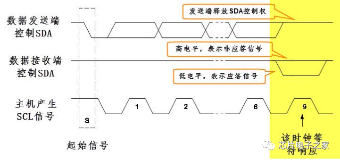
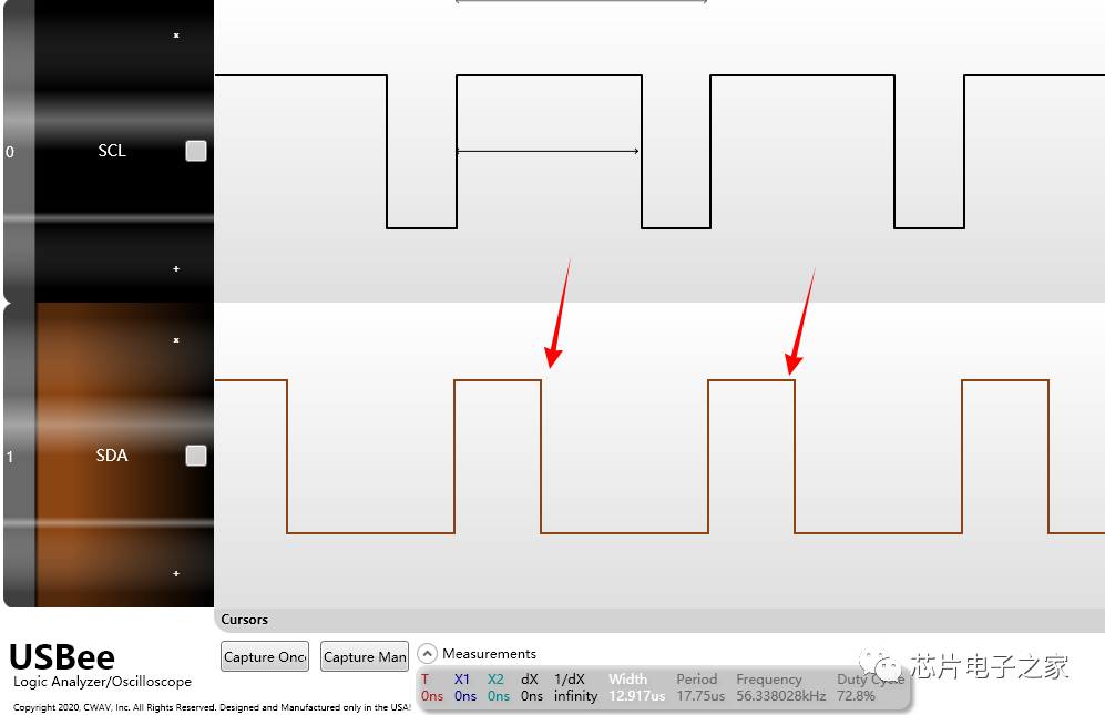
During transmission, the master generates the clock, and at the 9th clock cycle, the data sender releases control of the SDA, which is then controlled by the data receiver. If SDA is high, it indicates a not acknowledge signal (NACK); if low, it indicates an acknowledge signal (ACK).

One point not mentioned here is that the signal changes of SCL and SDA in the protocol have added delays. The minimum delay time must meet the standard requirements of the protocol;

Click below for keyword search

Reply with the keyword: “Join Group” to be added to the family group of Chip Electronics

(Disclaimer: This article is compiled for the purpose of disseminating relevant technical knowledge, and some collected materials are copyrighted by the original authors)

If you like it, please click “Read Again” at the end or share it to your “Moments“, so more people can learn!!! Thank youUsing Logic Analyzer to View Software Simulated I2C TimingUsing Logic Analyzer to View Software Simulated I2C TimingUsing Logic Analyzer to View Software Simulated I2C Timing
For more quality articles, please click on “Previous Highlights” below,Using Logic Analyzer to View Software Simulated I2C TimingUsing Logic Analyzer to View Software Simulated I2C TimingUsing Logic Analyzer to View Software Simulated I2C TimingUsing Logic Analyzer to View Software Simulated I2C TimingUsing Logic Analyzer to View Software Simulated I2C TimingUsing Logic Analyzer to View Software Simulated I2C Timing
☆ END ☆

Previous Highlights

▲Multisim Simulation Example Materials

▲Electronic Circuit Videos | Analog and Digital Electronics Learning Improvement

▲300 Sets of Electronic Circuit Analysis | Video Animated Tutorials

▲Switching Power Supply Video Repair Tutorial | 164 Series

▲Mini Program Development Technical Tutorial

▲Electronic Circuit Hardware Design Switching Power Supply Analog and Digital Design Video DIY Hard Tutorial

PCB Design Routing Details Explained (Text and Image Combined | Highly Recommended)

▲PCB&&||USB Differential Routing Experience and Lessons Learned

▲0 Ohm Resistor Usage Finally Summarized

▲PCB—The Role of Serpentine Lines, Explained

▲Should Power Inductors Have Copper Coverage?

▲Teaching You How to Design Schematics

▲Introduction to the Principles and Applications of Varistors, Discharge Tubes, Zener Diodes, and TVS

▲The Principles and Differences of DC-DC and LDO

▲Question: Why Does This Circuit Burn Out the MOSFET?

▲Reading Datasheets for Components, It Took Me a Long Time to Understand How to Read Them

▲Common Tips for Circuit Board Repair

▲MATLAB Made a Love Declaration Tool with Code

▲Introduction to the Principles of Lithium Battery Protection Boards

▲Essentials to Consider When Designing LDOs

▲Usage of Transistor and MOSFET Driver Circuits

▲How to Consider Analog Ground and Digital Ground in Circuit Design

▲Layout Considerations for Power Supply Boards

100 Knowledge Points on PCB Layout and Routing | Video Included

▲60 Essential Skills for Circuit Design

▲Detailed Explanation of Voltage Followers

▲MOSFET, Just Discussing How to Apply It

▲Design of Pyroelectric Infrared Sensor Amplifier Circuits

▲Deep Learning Switching Power Supply

▲Common Circuits for Voltage Comparators

▲12th Freescale | Remembrance

▲C Language | Unions, Structures

▲Design of a Pyroelectric Detection Circuit

▲Some Thoughts on Switching Power Supply Layout

▲STM32 Driving 16-bit ADC

▲Disassembly of Huawei Mobile Phone Power Supply #Process

▲Selection of Power Supply Chips

▲Precise Current Direction Analysis Starting from Capacitor and Inductor Formulas

▲Starting and Automatic Shutdown of LDO

▲Large Current Analysis Starting from Capacitor and Inductor Formulas

▲Microcontroller Driving MOSFET Circuit Applications

▲Differences Between Transistors and MOSFETs in Circuit Design

▲How to Make the 7805 Output Voltage Reach 10V

▲Switching Circuit to Achieve Crystal Oscillator Shutdown Function

▲How to Understand Input and Output Capacitors in LDOs

▲These Two Capacitors and Resistors in Switching Power Supplies

▲All Buffer Absorption Circuits in Switching Power Supplies

▲Tips for Using 10uF and 0.1uF Capacitors in Parallel

Leave a Comment