
The new RFSoC can reduce power consumption and package size by 50-75%, which is crucial for the efficient deployment of large-scale MIMO and millimeter-wave wireless backhaul for 5G.
Introduction
As the communications industry gradually aligns with 5G standards, mobile device manufacturers are keen on technology trials and proof-of-concept testing. Currently, the commercial viability of these technologies is undergoing rigorous evaluation; however, many of the technologies used in prototyping do not translate well into commercial deployment.
With the goal of increasing network capacity through lower power consumption, spectral efficiency, high densification, and new spectrum, manufacturers are relying on breakthroughs in software, hardware, and system-level technologies to achieve this goal.
Some technologies are critical to meeting stringent network capacity targets, and large-scale multiple-input multiple-output (MIMO) antenna arrays fall into this category. The RF units interfacing with these antenna arrays must meet extremely strict power consumption and package size requirements, but without breakthroughs in system integration, these targets are unlikely to be achieved.
Xilinx continues to play a major role in the realization, testing, and commercialization of pre-5G and 5G technologies, promoting flexibility and programmability in network design.
To make the commercialization of large-scale MIMO systems a reality, Xilinx is launching the industry’s first fully programmable RFSoC utilizing RF-level analog technology, which has made groundbreaking advancements in integration by perfectly integrating high-performance ADCs and DACs into the SoC. By replacing discrete data converters with integrated direct RF sampling technology, the RFSoC can reduce power consumption and package size by 50-75%, which is key for large-scale MIMO 5G radios and millimeter-wave wireless backhaul. Additionally, the combination of the SoC with direct RF signal processing provides comprehensive flexibility in the digital domain, bringing us closer to a commercially viable software-defined radio for wireless infrastructure.
The Key to 5G Commercial Deployment: Power Consumption and Package Size
Traditional 4G RF access networks (RAN) establish wired connections to remote RF units through high-loss coaxial cables. Although the remote RF architecture has evolved from 3G, it still faces several issues. The power consumption from the antenna to the remote RF unit remains very high, and the system size is large, making dense deployment unfeasible.
As shown in Figure 1, the next step in the evolution of RAN is to use active antenna arrays (bringing digital and analog RF units closer to the antennas) to save space, avoid cable losses and associated power consumption, while improving link budgets. Active antenna arrays were very successful in 4G but cannot meet the increased number of connected devices and user data rates in 5G.
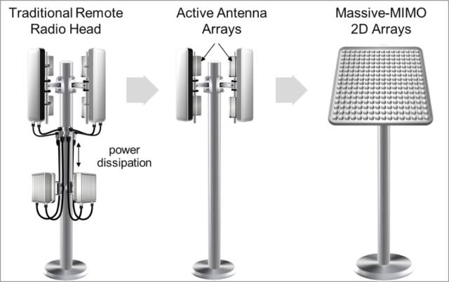
Figure 1 – Evolution of remote RF devices and antenna systems
Large-scale MIMO and beamforming technologies constitute a significant portion of the solution. As illustrated in Figure 1, a “large-scale” MIMO configuration can integrate 32, 256, or even up to 1024 independent [physical] antennas into a 2D array. Their phased array characteristics enable high-resolution beam control and lower power consumption, allowing for very high-density installations and significantly increasing capacity per unit. With this 2D array structure, new network topologies can be used in non-traditional layouts, including installations on building sides in a “tiled” manner or using irregularly shaped billboards or signs.
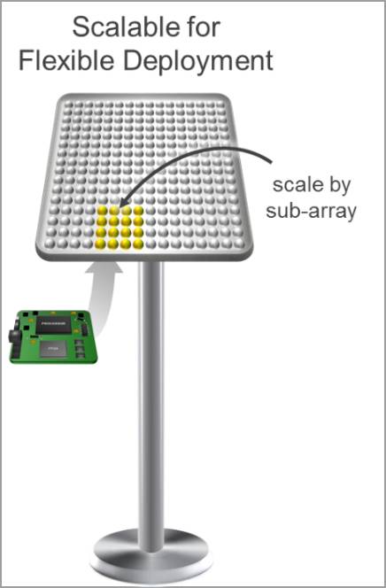
Figure 2 – Achieving flexible development through subsystem scalability
To support these large-scale MIMO arrays, remote RF units need to be compact and capable of supporting subarrays for flexible and scalable antenna configurations.
The Industry’s First All Programmable RFSoC
The All Programmable RFSoC addresses all of these issues. This device integrates communication-grade RF sampling data converters (with a digital processing subsystem), a stable and reliable ARM-level processing system, and FPGA architecture into a single chip. This represents a significant breakthrough in integration. In particular, the analog-to-digital signal chain is supported by a hardened DSP subsystem, facilitating flexible configuration for analog designers. This can reduce system power consumption and system size by 50-75%, achieving the necessary flexibility to adapt to evolving specifications and network topologies.
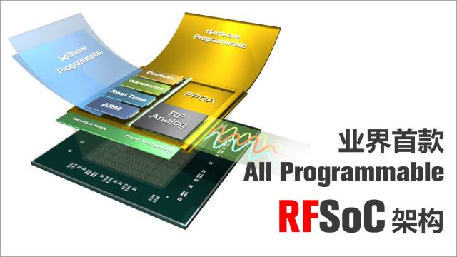
Figure 3 – Launching the first All Programmable RFSoC
Reducing Power Consumption, Package Size, and Design Cycle
Traditional radio systems consist of a processor, configurable logic, connection IP, and of course, data converters. When operating at high RF frequencies, the typical power consumption of a single-channel ADC is about 2W, while that of a DAC is about 1.25W. By reducing components through integration, power consumption and package size can be significantly reduced, which is particularly effective for high-channel-count systems. In addition to these advantages, integration can greatly simplify system design.
The main reason is that establishing connections with numerous discrete converters presents significant I/O challenges. To accommodate bandwidth expansion, most new converters use high-speed serial interfaces based on the JESD204B protocol, with rates up to 12.5Gb/s. This approach has many issues. First, implementing JESD204B IP cores takes time, consumes valuable FPGA resources, and incurs significant power consumption. Second, serial I/O power consumption increases significantly at higher data rates. However, the most challenging aspect is establishing serial links. Signal distortion at 12.5Gb/s is a problem, primarily due to high-loss low-cost copper cables used to run high line rates. This process is frustrating, and analog designers are eager for a solution.
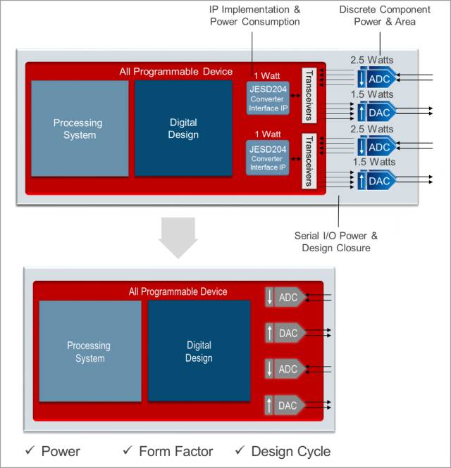
Figure 4 – Reducing power consumption, package size, and design cycle through integration
After integrating converters, there is no longer a need to use JESD204B IP cores and serial transceivers. The benefits are not limited to reducing power consumption and package size; they also significantly shorten development time.
Power Consumption Reduction of Up to 50%
Initial measurement results show a significant reduction in power consumption. In a typical 4 transmit, 4 receive (4Tx/4Rx) antenna configuration, the power consumption of discrete ADCs and DACs is significantly reduced, as shown in Table 1, with a 40% reduction in power consumption for an 8Tx/8Rx system.
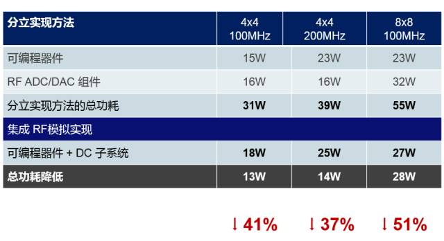
Table 1 – Reducing power consumption for digital radios (with DPD) through integrated subsystems
Package Size Reduction of Up to 75%
The degree of size reduction increases with the number of transceivers and antennas, as more converters can be avoided. In commercial devices, a typical RF ADC or DAC can occupy a footprint of up to 15x15mm per channel. The area savings in a 4Tx4Rx radio architecture is about 50%, and for larger radio architectures, such as the 8Tx/8Rx shown in Figure 2, the advantages become significantly greater, achieving over 75% area savings for fully deployed multi-channel systems. Considering that systems with multiple subarrays, such as 128Tx/128Rx, will be common in 5G, the area savings will be substantial. Given that individual antenna units are very small and usable area is limited, significant reductions in footprint are required for prototypes that need 10, 20, or more devices.
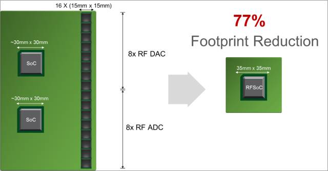
Figure 5 – Package size reduction in an 8Tx8Rx radio architecture
The Value of Direct RF Sampling
In addition to size, power consumption, and productivity advantages, another factor that cannot be underestimated is the inherent advantages of the converter subsystem based on leading direct RF sampling technology. This modern sampling method can sample incoming/outgoing RF signals “directly” without any prior signal conditioning with analog devices.
So far, most systems have adopted an analogized approach called intermediate frequency (IF or Zero-IF) sampling, which requires down-converting the raw signal to a sampling frequency supported by the ADC. Down-conversion circuits include mixers, high-quality oscillators, and other analog devices. Analog circuits are relatively inflexible and require highly specialized designs and complex device selections.
In direct RF sampling, incoming RF signals can be sampled directly without prior down-conversion. Once digitized, down-conversion and signal processing are completed in a more flexible programmable digital domain using digital signal processing techniques. These RF ADCs support higher sampling rates, and due to better filtering techniques in the digital domain, they can better balance dynamic range, signal quality (signal-to-noise ratio), and signal bandwidth.
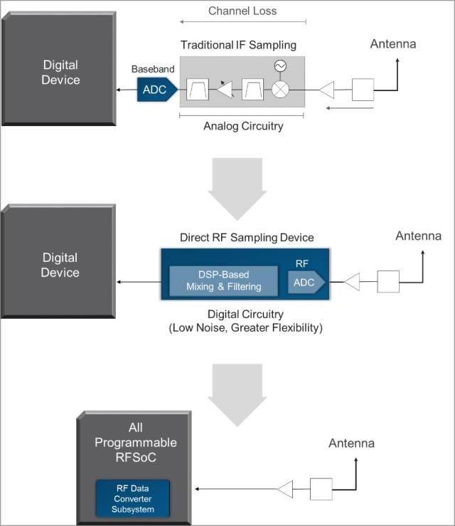
Figure 6 – Direct RF sampling and SoC integration
Xilinx takes this solution a step further through SoC integration, achieving complete flexibility in the digital domain while bringing radio processing closer to the antennas. By utilizing the same device to meet different Tx/Rx antenna configurations and evolving standards, mobile device manufacturers can respond quickly to market changes and opportunities. It is clear that in a 5G environment, no single type of radio technology can meet the diverse needs of next-generation radio access networks.
Complete Data Converter Subsystem for Flexibility
The RF data converter subsystem includes mixers, numerically controlled oscillators, decimation/interpolation, and other digital signal processing techniques for each channel—supporting complex signals for IQ processing. The converters possess the high sampling rates, large dynamic range, and resolution required for 5G. In some cases, digital down-conversion (DDC) does not require FPGA resources, and data goes directly into the logic architecture.
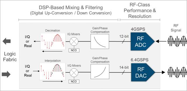
Figure 7 – Integrated RF subsystem in RFSoC
Comparison with Discrete RF Devices and Advantages of 16nm FinFET
Direct RF sampling is gradually being adopted. In fact, because IF sampling can enhance area and power efficiency, this traditional method is still widely used. These solutions are generally implemented on older chip processes (e.g., 65nm) and are low-cost. Given that the RF design community is more familiar with traditional analog usage models, this is likely the most suitable solution.
Discrete direct RF data converters, still considered “high-end,” are typically based on more advanced process nodes. While direct RF offers greater flexibility, the need for higher sampling rates means that discrete devices with rich digital processing capabilities may have power consumption disadvantages compared to analog implementations.
As shown in the figure below, although the independent flexibility advantages of direct RF sampling are real, the advantages become more apparent with the increase of discrete devices and trade-offs. Moreover, to achieve 5G, wireless manufacturers need more than just gradual improvements. For power consumption and size reduction, as well as flexibility, the most meaningful leap is full system integration. By combining the RF front end and radio front end into the same digital domain, system and analog designs become more flexible. In fact, integration makes RF sampling a more suitable technology for adoption, moving the industry closer to a fully software-defined radio.
Due to TSMC’s advanced 16nm FinFET process (which has excellent analog characteristics), the converter subsystem in RFSoC achieves outstanding unit power performance. By building the RF subsystem and the entire signal chain on advanced CMOS, RFSoC pioneeringly applies Moore’s Law to the analog domain.
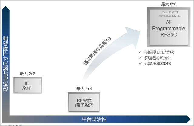
Figure 8 – Comparison of data converters for 5G wireless
Xilinx’s Experience in RF Analog Integration
High-performance ADCs/DACs were integrated into the 7 series FPGAs back in 2012—prior to RFSoC. Verified, characterized, and confirmed by customers, the test chips eliminated the JESD204 interface, demonstrating flexibility advantages, productivity advantages, and the ability to scale the number of channels. Proof of concept can guide application-focused All Programmable RFSoC development efforts.
Conclusion: Disruptive Technological Breakthroughs for the 5G Wireless Domain
With the launch of RF-level analog technology, Xilinx continues its mission of system integration. Whether at the chip level or system level, mobile manufacturers need breakthrough technologies to transition from oversized 5G test platforms and prototypes to smaller, commercially viable systems. In summary, RFSoC is timely, addressing urgent needs in 5G radio design.
Click below to read the original article for more exciting content