You’ve Come This Far
Don’t You Want to Know More?

Recently, I’ve seen many people in the industry asking how to verify CPUs and what SOC verification involves. Today, I will briefly introduce IP, FPGA, SOC, and CPU verification.
A typical chip team is composed of several departments: the Architecture department, IP designer department, IP DV department, Analog department, SOC integrator department, SOC DV department, DFT department, PD department, and Firmware department. In larger companies, there may also be a CPU department and a CPU DV department. If we include the FPGA verification handled by the Firmware department, verification (DV) occupies a significant part of a chip design company.
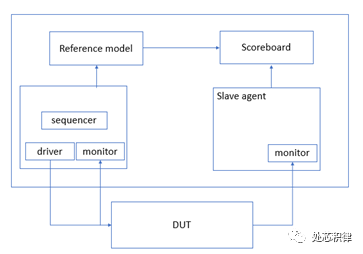
First, let’s introduce IP verification. IP stands for Intellectual Property in English. In the chip industry, functional modules developed by chip design engineers are considered a form of intellectual property. We can understand IP as modules that implement certain functionalities, such as AXI, AHB, USB, PCIE, DDR, etc. The primary responsibility of IP verification engineers is to ensure that these functional modules work correctly. The verification methods employed by IP verification engineers mainly include UVM verification, Formal verification, and sometimes C. A typical verification model is generally illustrated as follows:
IP verification can be further divided into algorithmic verification and protocol verification, with similar methods employed for both. Currently, the focus is still on coverage convergence. The primary tasks of IP verification engineers include:
a. Reading specifications and listing test plans (testplan);
b. Designing the verification environment architecture and setting up the verification environment;
c. Designing test cases based on the test plan;
d. Collecting code coverage and function coverage;
e. Testing IP performance.
The above five points outline the main responsibilities of IP verification engineers. Some companies may also involve IP verification engineers in power consumption testing, FPGA verification, and SOC verification.
FPGA verification refers to the process of synthesizing the design into a bitfile and programming it onto an FPGA platform for testing. The FPGA verification work is primarily led by the Firmware department. In a mature process, FPGA verification may even be unnecessary; theoretically, issues that can be detected by FPGA can also be caught through IP DV. The downside of FPGA is that debugging can be quite cumbersome, but due to its rapid execution, FPGA is more focused on high-frequency stress testing compared to IP DV, meaning repeated testing of a particular scenario or many scenarios multiple times.
Many companies hope to achieve the simulation speed of FPGA while being able to intuitively pull waveforms for debugging. Existing solutions include developing hardware accelerators, represented by Cadence’s Palladium and Synopsys’s ZEBU. There are also efforts to accelerate simulation speed through cloud computing, with domestic startups researching in this area. Additionally, some foreign companies combine FPGA with dynamic simulation, such as Smart DV SimXL. If you want to know more about this knowledge, you can search online; we won’t elaborate further here.
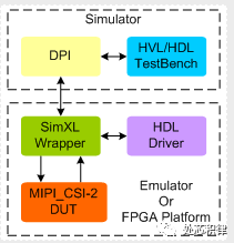
Image source: Smart DV
What does SOC verification mainly involve? SOC stands for System On Chip. The SOC verification engineer’s verification object is the entire chip design, which is a crucial position to ensure the normal operation of the entire chip’s functionality. SOC verification focuses more on system-level connections, power management, the collaboration of multiple modules (cores), and system-level performance testing. Sometimes, SOC DV will also collaborate with the Firmware department for software debugging.
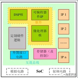
Image from Baidu Encyclopedia
SOC verification methods primarily involve writing C/asm software code to complete a series of test cases, then using a toolchain to compile the C/asm code into binary files placed in RAM/flash. The CPU reads the data from RAM/flash to execute relevant instructions to control external memory and peripherals. The entire process simulates the actual operation of a chip. The work includes the following:
c. Testing the integration of various IPs on SOC;
d. Testing bus interconnections;
e. Testing various clocks and resets (clock switching/frequency modulation, software/hardware resets, etc.);
f. Power management testing;
h. Power consumption testing (e.g., PTPX);
i. Power connectivity-related testing (UPF/CPF testing);
j. Netlist functionality testing (Postsim);
In addition to using C for SOC verification, some also utilize UVM and Formal. When a chip exceeds 20 million gates, SOC verification engineers may also run emulation, using ZEBU or Palladium to verify the functionality and performance of the entire chip.
CPU verification is relatively unfamiliar to most people, mainly because there are few companies that develop CPUs themselves. Currently, RISCV is developing rapidly, with many companies integrating their functions into SOCs using extended instructions for control, thus necessitating modifications to CPUs. Future demand for CPU verification may increase. The methodology for CPU verification differs slightly from that of IP verification, with primary verification methods including software self-testing, using a random instruction generator (ISG) combined with an instruction simulator (ISS) for verification, and using Formal verification.
Software self-testing involves running a program and comparing the results with the expected outcomes. For example, during a multiplication operation, the program compares the CPU’s computed result with the pre-stored result.
The testing using ISG and ISS involves generating random instructions through ISG, executing the random instruction program on the CPU, and simultaneously executing the same program on ISS. Finally, the trace logs generated by the CPU execution and those by ISS are compared to determine if the CPU executed the instructions correctly. The verification framework is generally illustrated as follows:
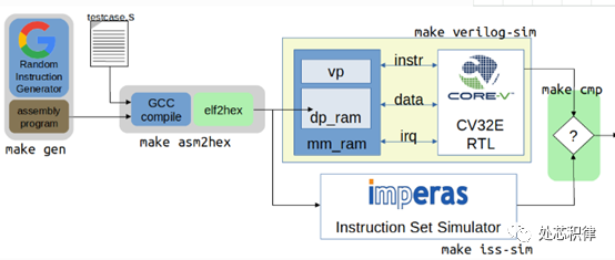
Image from openhw website
Currently, a classic ISG used is Google’s ISG, and some companies implement ISG using UVM. If you want to extend the RISCV instruction set, both ISS and ISG need to be developed by yourself.
Historical Recommendations
IC Verification Engineer’s Efficient Combat Manual — What to Pay Attention to When Building an Efficient Verification Platform and Smoke Testing?
IC Verification Engineer’s Efficient Combat Manual — Sorting Verification Feature Documents
Learning Design Patterns with IC Verifiers (1) — Singleton Pattern
How to Call Functions in Agents Within Sequences and Quickly Experiment with Your Ideas?
Discussing Interrupt Verification (1) Common Mistakes Made by Verification Engineers (4) — Sign Bit Extension Issues
Your Clicks Are Encouragement for Us