
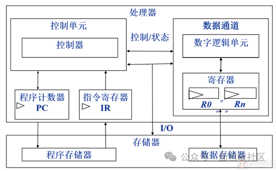
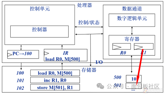
Fetch: Obtain the next instruction to be executed from memory into the instruction register; PC: Program Counter, always points to the next instruction to be executed; IR: Instruction Register, used to hold the fetched instruction; as shown in the figure:
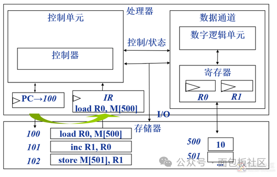
Decode: Interpret the instruction, determine the meaning of the instruction execution; as shown in the figure:
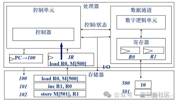
Execute: Move data from memory to the data channel register; perform data operations through the arithmetic logic unit ALU; as shown in the figure:
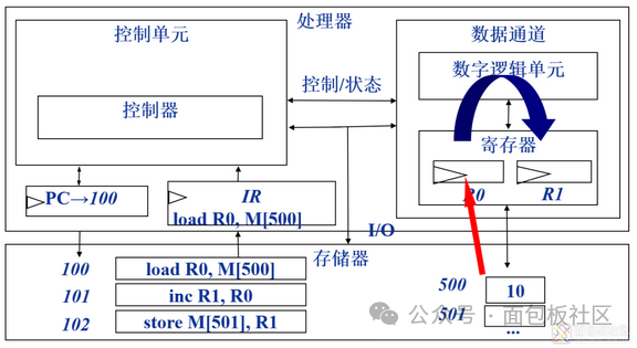
Store: Write data from the register to memory. As shown in the figure:
On some microprocessors, such as ARM series processors, DSPs, etc., the instruction implementation uses pipelining, and the instruction process is divided according to the number of pipeline stages. For example, a 5-stage pipeline processor will execute instructions in 5 phases.
(1) By storage structure: von Neumann architecture and Harvard architecture
Von Neumann architecture, also known as Princeton architecture, is a memory structure that combines program instruction memory and data memory. The processor accesses program and data memory via the same bus, with the same width for program instructions and data. Examples include the X86 series, ARM7, etc. as shown: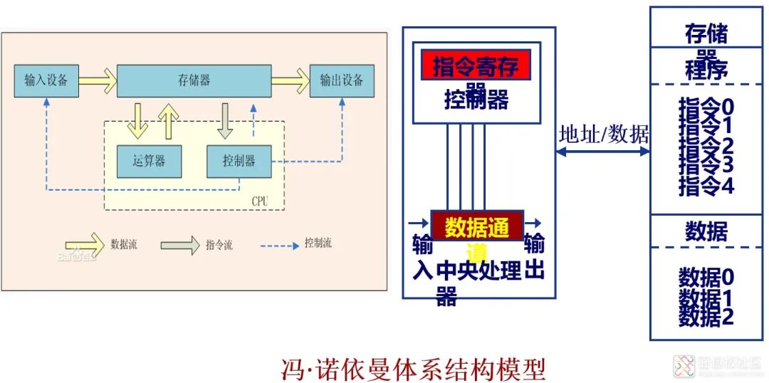
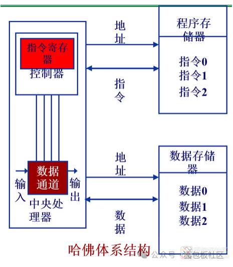
Harvard architecture is a memory structure that separates program instruction storage and data storage, aimed at alleviating memory access bottlenecks during program execution. Microprocessors with Harvard architecture typically have higher execution efficiency. Examples include Microchip’s PIC series chips, Motorola’s MC68 series, Zilog’s Z8 series, ATMEL’s AVR series, and ARM’s ARM9, ARM10, and ARM11. As shown:
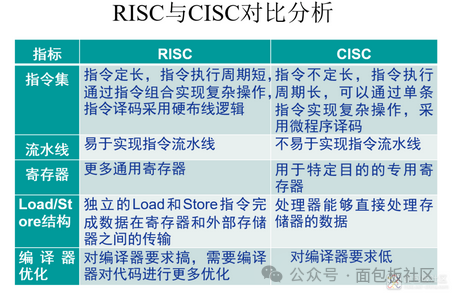
By instruction type, it can be divided into: Complex Instruction Set (CISC) processors and Reduced Instruction Set (RISC) processors. CISC: Complex Instruction Set Computer; has a large number of instructions and addressing modes, requiring more interpreters.
80/20 rule: 80% of programs only use 20% of instructions;
The majority of programs can run using only a small number of instructions.
CISC has the following significant characteristics: (1) Instruction format is not fixed, instruction length is inconsistent, operands can be many or few; (2) Addressing methods are complex and varied, facilitating program writing; (3) Uses microprogramming architecture, executing each instruction requires completing a sequence of microinstructions; (4) Each instruction requires several machine cycles to complete; the more complex the instruction, the more machine cycles it consumes. RISC: Reduced Instruction Set Computer: has fewer instructions, only contains the most useful instructions in the channel; short execution time ensures that the data channel quickly executes each instruction; simplifies CPU hardware design; each instruction uses a standard word length.

ARM stands for Advanced RISC Machines.
On April 26, 1985, the first ARM prototype was born at Acorn Computers Ltd. in Cambridge, UK.
In the late 1980s, ARM quickly developed into Acorn’s desktop product, forming the basis of computer education in the UK.
In 1990, Advanced RISC Machines Limited was established.
In the 1990s, the ARM 32-bit embedded RISC (Reduced Instruction Set Computer) processor expanded globally, occupying a leading position in the low-power, low-cost, and high-performance embedded system application fields.
It now holds over 75% of the 32-bit embedded product market.
The 32-bit RISC processor is favored, with ARM embedded microprocessor series leading the way.
Although ARM was established only over 20 years ago, in 1999, due to the booming mobile phone market, its 32-bit RISC processor accounted for more than 50% of the market share, and by early 2001, ARM’s 32-bit RISC processor market share exceeded 75%. ARM is an intellectual property supplier and design company. Partner companies produce uniquely designed chips.
Features of ARM processors: (1) ARM instructions are 32-bit fixed length (except for the AArch64 architecture, which adds 64-bit instructions); (2) Rich in registers (37 registers); (3) Ordinary Load/Store instructions; (4) Multiple register Load/Store instructions; (5) Conditional execution of instructions; (6) Single instruction completes data shift operation and ALU operation in a single clock cycle; (7) Extend the functionality of ARM processors through variants and coprocessors; (8) Extend the 16-bit Thumb instructions to improve code density. The naming rules of ARM are roughly divided into two categories: “Processor Series” naming rules based on ARM Architecture version; “Processor Model” naming rules based on ARM Architecture version.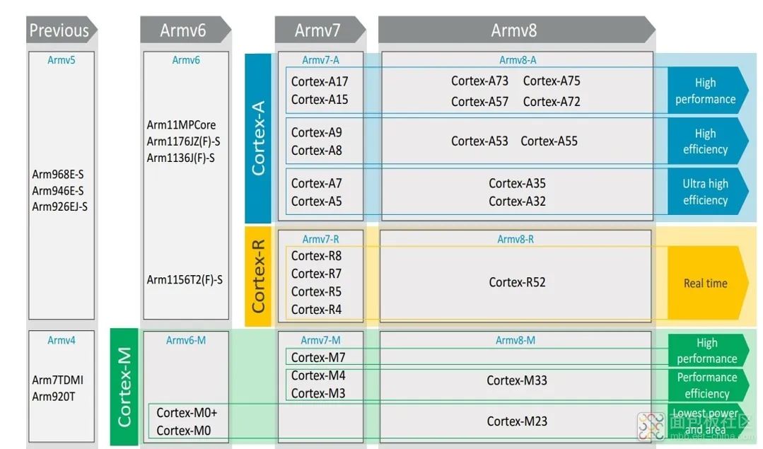

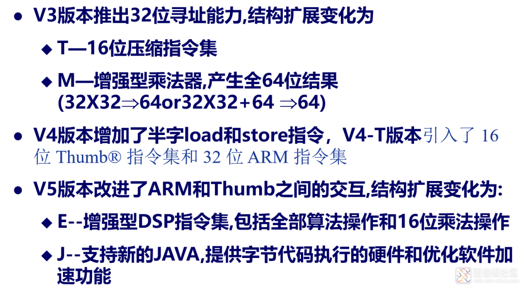
ARMv6 architecture introduces a series of new features including Single Instruction Multiple Data (SIMD) operations.
ARMv6-M architecture is designed for low-cost, high-performance devices, providing a powerful 32-bit solution to markets previously dominated by 8-bit devices, such as Cortex™-M0 and Cortex-M1. The ARMv7 architecture, all ARMv7 architecture processors implement Thumb-2 technology (an optimized 16/32-bit mixed instruction set), divided into three types of processors: Cortex-A – application processors, Cortex-R – real-time processors, Cortex-M – microcontrollers.
ARMv8 architecture, ARMv8-A introduces 64-bit architecture support into the ARM architecture, including: 64-bit general registers, SP (stack pointer) and PC (program counter), 64-bit data processing and extended virtual addressing, compatible with 32-bit processing.
ARMv9 architecture, the most significant upgrade lies in AI and security, enhancing security based on ARMv8, adding capabilities in vector computing, machine learning, and data signal processing, and greatly improving performance. 1) ARM Data Types (1) Double Word: 64 bits (2) Word: In ARM architecture, the word length is 32 bits. (3) Half Word: In ARM architecture, the half word length is 16 bits. (4) Byte: In ARM architecture, the byte length is 8 bits.
2) ARM Processor Storage Format
As a 32-bit microprocessor, the maximum addressing space supported by the ARM architecture is 4GB.
The ARM architecture can store word data in two ways: big-endian and little-endian.
Big-endian (high to low): the high byte of the word is stored in the low address byte unit, and the low byte of the word is stored in the high address byte unit.
3) ARM Processor Operating States
From a programming perspective, the ARM microprocessor generally has two operating states, ARM and Thumb, and can switch between the two states.
(1) ARM state: At this time, the processor executes 32-bit word-aligned ARM instructions, most of the work is done in this state. (2) Thumb state: At this time, the processor executes 16-bit half-word-aligned Thumb instructions.
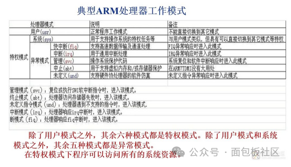
THUMB instruction characteristics: THUMB code occupies 70% of the space required by ARM code; THUMB code uses 40% more instructions than ARM code; using 32-bit storage, ARM code is 40% faster than THUMB code; using 16-bit storage, THUMB code is 45% faster than ARM code; using THUMB code, external storage power consumption is 30% less than ARM code. 4) ARM Processor Operating Modes
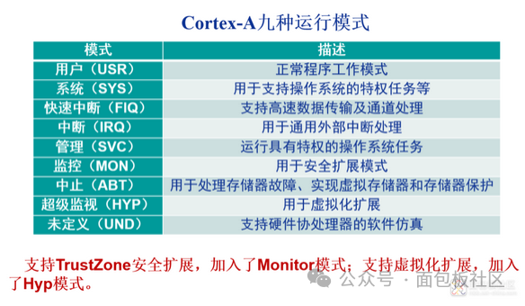
5) ARM Cortex-A Processor Operating Modes
6) Cortex-A Register Group
34 general-purpose registers, including R0-R14 in various modes and the shared R15 program counter (PC), all of which are 32 bits. 8 status registers, with one ELR_Hyp register unique to Hyp mode.
7) Program Status Registers CPSR and SPSR
Like other processors, ARM has program status registers to configure processor operating modes and display operating states. ARM processors have two program status registers, CPSR (Current Program Status Register) and SPSR (Saved Program Status Register).
CPSR can be accessed in any running mode, including condition flags, interrupt disable bits, current processor mode flags, and other relevant control and status bits.
Each running mode has a dedicated physical status register, known as SPSR for the status register.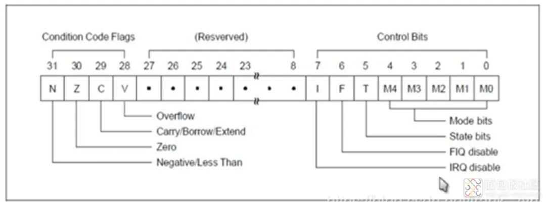
(1) N (Negative): When performing operations with signed numbers represented in two’s complement, N=1 indicates the result is negative, N=0 indicates the result is positive or zero. (2) Z (Zero): Z=1 indicates the operation result is 0, Z=0 indicates the operation result is non-zero. (3) C (Carry): There are 4 ways to set the value of C:
1) Addition instruction (including comparison instruction CMP) 2) When the operation produces a carry (unsigned overflow), C=1, otherwise C=0 3) Subtraction operation (including comparison instruction CMP) 4) When the operation produces a borrow (unsigned overflow), C=0, otherwise C=1
For non-add/subtract operation instructions that include shift operations, C is the last bit of the value shifted out. For other non-add/subtract operation instructions, the value of C usually remains unchanged.
(4) V (Overflow): There are 2 ways to set the value of V: 1) For add/subtract operation instructions, when the operands and the operation result are signed numbers represented in binary’s two’s complement, V=1 indicates a sign bit overflow. 2) For other non-add/subtract operation instructions, the value of V usually remains unchanged.
(5) I (Interrupt Request): I=1 indicates that IRQ response is disabled, I=0 indicates that response is allowed. (6) F (Fast Interrupt Request): F=1 indicates that FIQ response is disabled, F=0 indicates that response is allowed. (7) T (Thumb): T=0 indicates the current state is ARM state, T=1 indicates it is Thumb state. (8) M4-M0: Indicates the current processor’s working mode.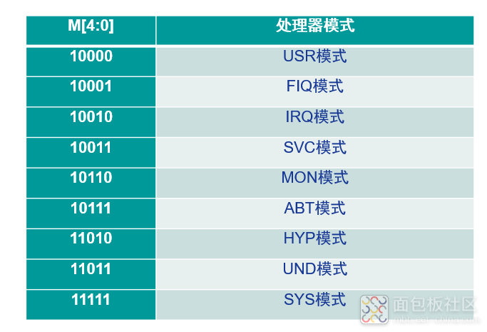
8) Conditions for Switching Operating Modes
(1) Execute a software interrupt (SWI) or reset command (Reset) instruction. If the SWI instruction is executed in user mode, the CPU enters supervisor mode. (2) An external interrupt occurs. If an external interrupt occurs, the CPU will enter IRQ or FIQ mode. (3) An exception occurs during CPU execution. The most typical exception is a memory access exception caused by MMU protection, at which point the CPU will switch to abort mode. If it is an invalid instruction, it will enter undefined mode. (4) There is a mode that the CPU cannot enter automatically, which is the system mode; to enter system mode, the programmer must write an instruction to achieve it. To enter system mode, simply change the CPSR mode bit to the corresponding mode bit for system mode. (5) In any privileged mode, other modes can be entered by modifying the CPSR’s MODE field. However, it should be noted that the modified CPSR is the shadow CPSR in that mode, i.e., SPSR, so it is not the actual CPSR; therefore, the general practice is to modify the shadow CPSR and then execute a MOVS instruction to restore execution at a breakpoint and switch to the new mode.

1) What is Memory Mapping
Memory mapping refers to the mapping from virtual addresses to actual physical addresses implemented by the Memory Management Unit (MMU) in the ARM storage system, as shown in the figure.
2) Why Memory Mapping
The A32 architecture of ARM has a 32-bit address bus, so the CPU can address a range from 0x00000000 to 0xffffffff, with an addressing space of 4GB. All internal and external storage or peripheral units need to be operated through corresponding addresses, and the types and quantities of different chip peripherals vary in addressing space. To enable the kernel to manage different chip designs more conveniently, the ARM kernel provides predefined storage mappings.
Chip design companies need to define the internal peripherals and external reserved interfaces of the chip based on the predefined memory mapping provided by the kernel. The benefit of this approach is that it greatly reduces the trouble of address conversion between different chips with the same kernel (the CPU operates on a unified virtual address, while the actual physical address is managed by the MMU).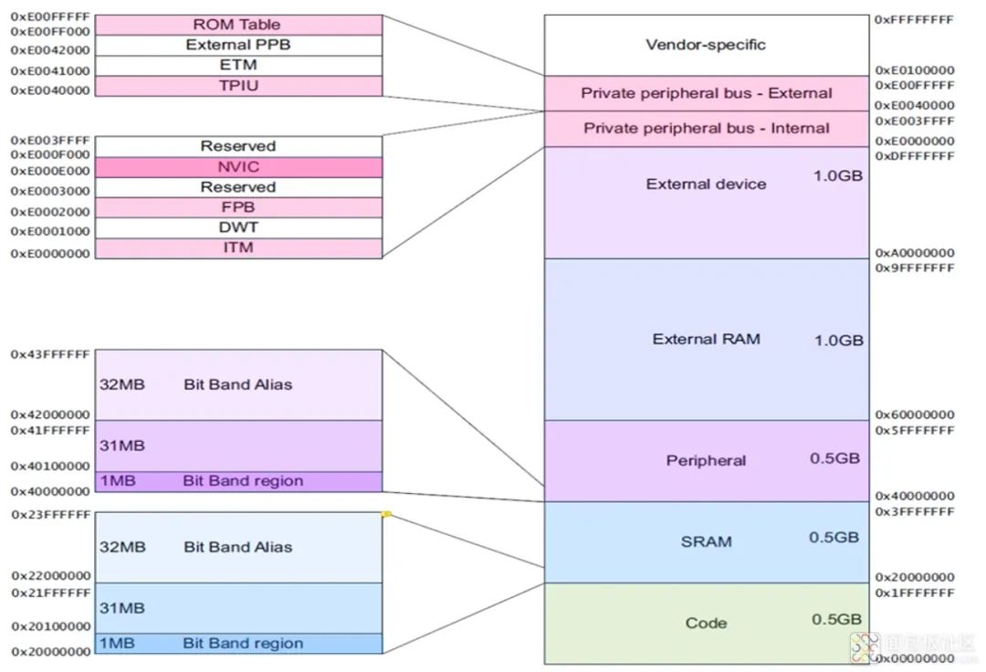
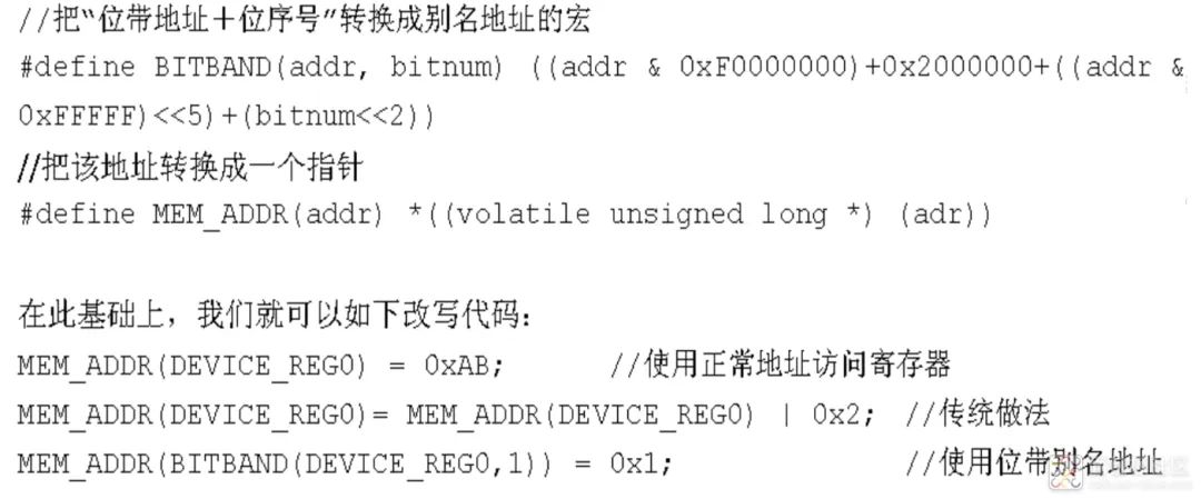
3) Bit-Banding Operations
(1) What is Bit-Banding Operation? A simple example is that when using a 51 microcontroller to operate P1.0 to a low level, we know that this actually involves writing 1 or 0 to a certain bit in a register. However, during CPU operations, each address corresponds to an 8-bit byte. How can we directly operate on one of the bits? This is where bit-banding operations come into play.
(2) Which addresses can perform bit-banding operations? The above figure shows two areas where bit-banding is implemented. One is the lowest 1MB range of the SRAM area (Bit band region), and the other is the lowest 1MB range of the on-chip peripheral area. 4) Register Address Calculation
In ARM, all peripheral addresses are generally mounted on the AHB or APBx bus, so we often use the base address + offset address + structure method to quickly and clearly calculate the specific register address of a peripheral, as shown in the figure.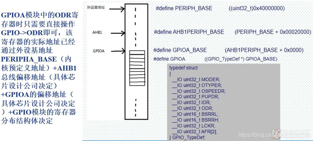
5) Integrated Peripheral Register Access Methods
Source: Breadboard Community User czd886 shares
END
Electronic Engineer DIY Creative Design Competition
Event Time: 2023.11.1-2024.1.15

Award Settings: First Prize (1): Uni-T UTD1025CL Handheld Digital Storage Oscilloscope/DJI Osmo Action 4 Gimbal Sports Camera/DJI Mini 2 SE Drone (choose one)
Second Prize (2): Xiaomi Redmi Pad SE tablet one. Third Prize (3): Pro’sKit SS-936H Temperature Controlled Soldering Station Set. Participation Prize (10): 100 yuan JD card (based on the participating works, difficulty, etc.)
 Click to read the original text to participate in the activity!