Surface Defects of LCD Panels and Detection Methods

With the rapid development of the new generation of information and communication technology, the market demand for terminal devices such as smartphones, tablets, and smart home products continues to grow, leading to a sharp increase in the production scale of LCD panels, making them one of the pillars of the information industry.
The rise of the LCD panel industry has driven a surge in demand for panel quality inspection.
Traditional defect detection is mainly done by human eyes, which poses significant challenges for enterprises in controlling production quality and improving production efficiency. Given this, adopting a new type of panel quality inspection method to replace manual inspection is an urgent technical problem to be solved.
Surface Defects of LCD Panels and Detection Methods
01 Origins of LCD Panel Defects
Thin-film transistor liquid crystal displays (TFT-LCD) have advantages such as high resolution and low power consumption, which is why they are widely used in the display industry.
However, due to the complex production processes and environmental factors, it is difficult to avoid defective displays, leading to a high product defect rate. The manufacturing of TFT-LCD displays involves processes such as coating, etching, developing, panel assembly, encapsulation, and installation of driver chips, with complex procedures leading to defects. Common defects include point defects, line defects, and Mura defects.
The term “Mura” comes from Japanese, meaning spots or stains, and is also known as “cloud spots.” It is one of the most challenging defects to detect in displays. Traditional Mura detection methods are implemented through manual visual inspection, primarily relying on naked-eye identification. This method is inefficient and prone to visual fatigue, resulting in reduced accuracy of results.
Machine vision-based detection of LCD panels can effectively detect defects arising from various production processes, including array processes, CF (color filter) processes, CELL (cell assembly) processes, and module processes, enabling effective detection and differentiation of defects such as cracks, breaks, chips, scratches, burrs, and drops.
Surface Defects of LCD Panels and Detection Methods
02 Challenges in LCD Panel Detection

Large product area and high production capacity make it impossible for manual inspection of every panel, posing a risk of missed detections.

Before cutting, LCD panels typically have a large area. For example, a 10.5-generation line can have a panel area of up to 3370mm*2940mm, making manual inspection extremely difficult and prone to fatigue, thus failing to ensure production capacity and accuracy.

Panel defects can easily lead to product breakage.

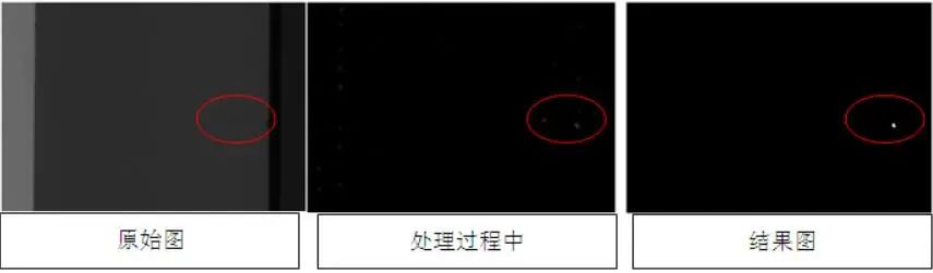
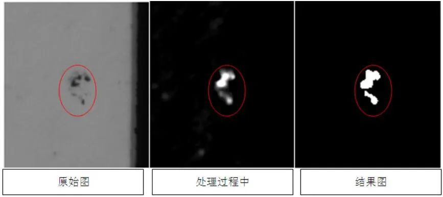
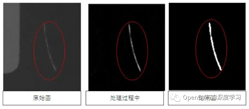
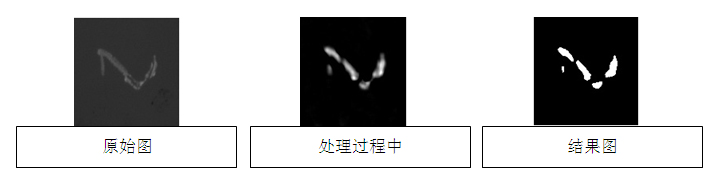
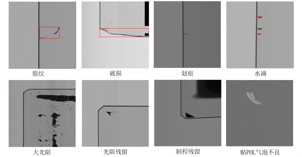
During the production of LCD panels, defects such as edge chipping, breakage, cracks, and scratches may occur. If not detected and addressed promptly, they can lead to glass breakage within the main production equipment in subsequent processes, necessitating downtime for maintenance and cleanup, resulting in economic losses.

The locations and types of defects cannot be statistically analyzed or digitized.

Manual inspection lacks image documentation, leading to poor consistency in detection standards and hindering product traceability.

Difficulty in recruitment and high labor costs.

As the average wage level continues to rise, labor costs increase annually, and recruitment becomes challenging due to high employee turnover. Additionally, manual inspection poses significant harm to workers’ eyes, resulting in high turnover rates and recruitment difficulties.

03 LCD Panel Detection Methods
In recent years, many computer vision-based panel defect detection systems have emerged, but the detection algorithms used by various manufacturers are mostly traditional visual methods. However, with the continuous advancement of production processes, detection requirements have increased, along with the demand for higher precision and real-time performance of algorithms.
With the rise of deep learning, we utilize convolutional neural networks (CNN) to detect hard-to-detect defects on screens.
Regarding detection issues, there are many existing object detection algorithms that can achieve high precision and real-time detection, effectively identifying and classifying defects in LCD panels—detecting defects such as edge chipping, cracks, stains, drops, and scratches, and integrating with the main production equipment for automatic feedback based on the type of defect: either stopping the machine or triggering an alarm, without the need for real-time monitoring by staff on site.
Surface Defects of LCD Panels and Detection Methods

Increase Efficiency

Deep learning algorithms can more accurately identify production hazards such as edge chipping, thus preventing production line downtime caused by glass fragments and eliminating false alarms caused by misidentification, thereby improving production efficiency.

Reduce Costs

Avoid damage to equipment caused by glass breakage, reduce the costs associated with downtime, and lower repair costs for equipment.

Improve Quality

Reduce product quality issues caused by surface scratches and stains affecting circuit production and liquid crystal imaging.

Enhance Processes

By digitizing quality inspection, enhance data traceability and analysis capabilities, providing strong support for improving production processes.

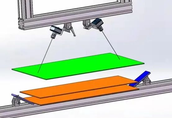
LCD Screen Appearance Defect Detection Scheme

Surface Defects of LCD Panels and Detection Methods
Using line array cameras and lenses, select backlight sources, coaxial light, or high-brightness line light sources based on detection requirements to capture images of the LCD panel. During the image scanning process, intelligent algorithms simultaneously process the images, displaying defect information in real-time, determining whether there are foreign objects, scratches, discoloration, bulges, dents, pinholes, burrs, or bright spots on the surface. For defective glass, real-time linkage with the main equipment is performed to stop operations and prevent downtime due to glass breakage during production.
Machine Vision Detection Process Design:
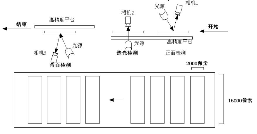
1. Open the product to 180°, placing the LCD screen horizontally on the stage;
2. Start detection: the stage moves, and the camera begins to capture images;
3. After capturing, the stage resets;
4. Detection software analyzes the quality of the LCD screen;
5. Based on the analysis results, provide OK or NG judgment results for the product;
6. Operator: performs sorting and re-inspection based on the results;
A) Visual Detection Anomaly: Black Spot
Surface Defects of LCD Panels and Detection Methods
B) Visual Detection Anomaly: Foreign Object
Surface Defects of LCD Panels and Detection Methods
C) Visual Detection Anomaly: Scratch
Surface Defects of LCD Panels and Detection Methods
D) Visual Detection Anomaly: Bubble
Surface Defects of LCD Panels and Detection Methods
E) Visual Detection Anomaly: Foreign Object
Surface Defects of LCD Panels and Detection Methods
This article is sourced from: Machine Vision Salon, for academic sharing only. If there is any infringement, please contact us to delete the article.

Leave a Comment