In today’s rapidly advancing technological era, chips have become the “heart” driving the digital world. From smartphones to data centers, from new energy vehicles to 5G base stations, ubiquitous chips are becoming smaller and faster. To break through physical limits and meet the increasing integration requirements of Moore’s Law, semiconductor manufacturing is shifting from traditional “coarse processing” to precise “atomic-level craftsmanship.” Among these, Atomic Layer Etching (ALE), Neutral Beam Etching (NBE), and Atomic Layer Deposition (ALD) are the three core technologies that are becoming crucial for the manufacturing of the next generation of semiconductor devices, especially for the third generation semiconductor GaN HEMT (High Electron Mobility Transistor).
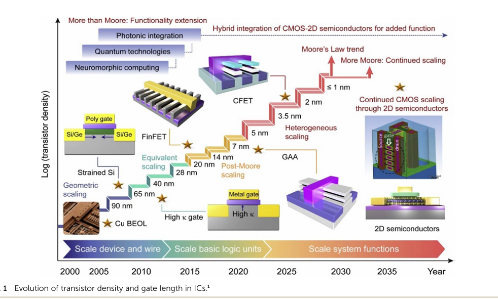
1. The Challenge of Moore’s Law: The Leap from “Macro” to “Atomic”
Traditional semiconductor manufacturing relies on techniques such as wet etching and dry etching. Wet etching is cost-effective and highly selective, but it is difficult to precisely control feature sizes smaller than 1 micron and carries contamination risks. On the other hand, dry etching, while offering higher precision to define fine structures, can cause surface damage and radiation defects due to its plasma processes.
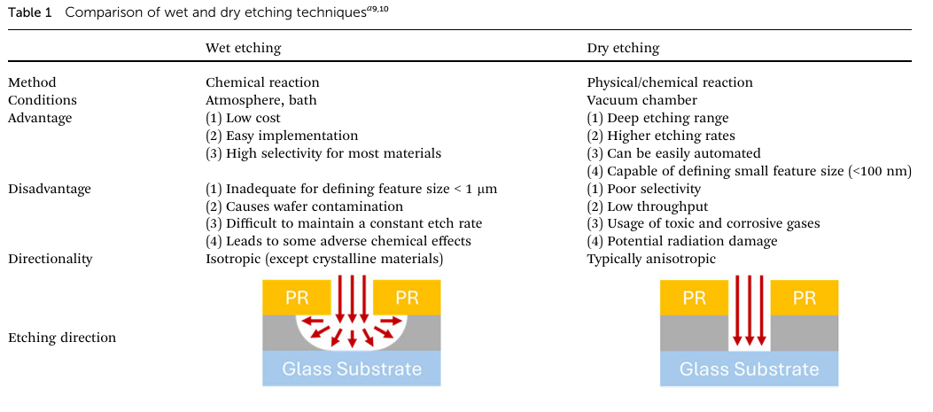
As transistor sizes continue to shrink, especially at 5-nanometer and more advanced process nodes, the complexity and precision requirements of the processes are increasing exponentially. Even minor etching depth or profile deviations can significantly affect device performance, leading to threshold voltage shifts, increased leakage current, and decreased drive current. To address these challenges, semiconductor manufacturing needs to introduce ultra-precise and ultra-fine new technologies, namely Atomic Layer Etching (ALE), Neutral Beam Etching (NBE), and Atomic Layer Deposition (ALD). These technologies, with their atomic-level precision in thin film growth and removal, have become the cornerstone for ensuring device performance and reliability.
2. Atomic Layer Etching (ALE): The Art of Precise “Onion Peeling”
Atomic Layer Etching (ALE) is a high-precision technology capable of removing materials layer by layer. Its working principle is akin to “peeling an onion,” ensuring that each cycle removes only one atomic layer through a series of self-limiting reactions. This minimizes the risk of over-etching and reduces surface roughness.
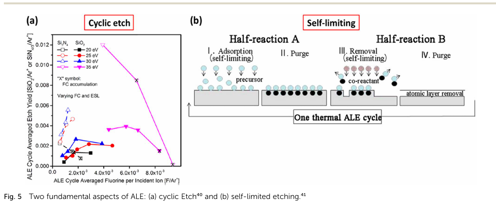
ALE is mainly divided into two mechanisms: thermal ALE and plasma ALE. Thermal ALE utilizes chemical reactions to form volatile compounds, selectively removing surface layers in a self-limiting process. Plasma ALE, on the other hand, uses plasma to activate surface reactions, providing additional energy suitable for materials requiring higher temperatures or complex precursors.
A typical ALE cycle usually includes four steps:
-
Introduction of Reaction Gases: Reactive gases (such as chlorine) are introduced to the surface, adsorbing onto the material to be etched.
-
Purging: Excess reaction gases are purged to prevent unnecessary reactions.
-
Ion Source Activation: Ion source gases (such as argon) are introduced to activate the plasma, providing energy to remove the adsorbed material layer.
-
Final Purging: By-products of the etching reaction are cleared away.
It is this cyclical self-limiting process that ensures atomic-level precision. In the manufacturing of GaN HEMT, the application of ALE is particularly critical. It can control the gate recess depth with atomic-level precision, which is essential for accurately controlling the device’s threshold voltage (Vth).
3. Neutral Beam Etching (NBE): The Gentle Yet Powerful “Scalpel”
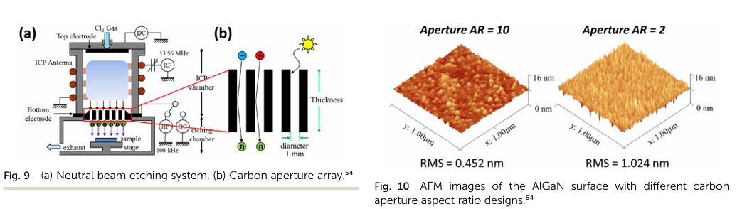
Traditional plasma etching generates charged particles (ions) and ultraviolet photons, which can damage semiconductor devices. In contrast, Neutral Beam Etching (NBE) uses neutral particle beams for etching, perfectly avoiding the common issues of charge accumulation and radiation damage found in traditional plasma etching, making it particularly suitable for etching delicate structures like GaN-based semiconductors.
The advantages of NBE are especially evident in the manufacturing of GaN HEMT. Studies have shown that compared to traditional plasma beam (PB) etching, NBE etching reduces the isolation leakage current of GaN HEMT by tenfold (from 1 µA mm⁻¹ to 0.1 µA mm⁻¹). Surface roughness is also significantly improved, indicating that NBE can produce more reliable and better-performing GaN HEMT devices.
4. Atomic Layer Deposition (ALD): Perfectly “Dressing” the Film
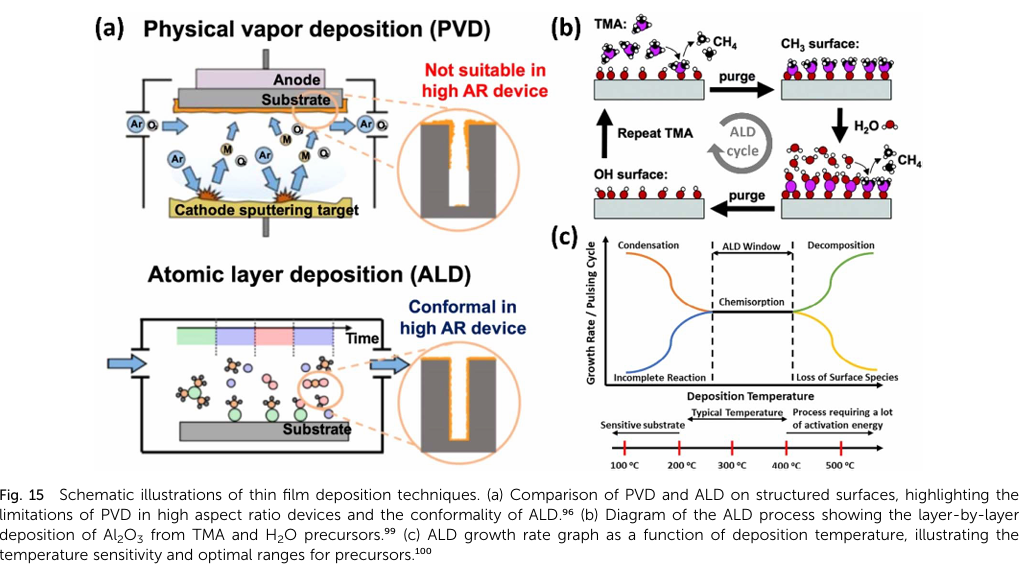
In contrast to etching, Atomic Layer Deposition (ALD) is a technique that can precisely grow films to the atomic layer level. It achieves excellent control over film thickness and uniformity by alternately introducing different precursors and utilizing self-limiting surface reactions.
ALD is also crucial in the manufacturing of GaN HEMT. For example, ALD is commonly used to deposit high-k gate dielectric layers, such as HfO₂ and Al₂O₃, on GaN devices. These materials can effectively increase gate capacitance while significantly reducing leakage current. In GaN HEMT, a high-quality gate dielectric layer is essential for achieving low gate leakage, high transconductance, and excellent dynamic on-resistance characteristics. The superior conformality provided by ALD ensures that these films can perfectly cover complex three-dimensional structures.
5. Deep Integration: The “Golden Combination” in GaN HEMT Manufacturing
ALE, NBE, and ALD do not exist in isolation; their combined application is driving innovation in advanced semiconductor manufacturing. Particularly for emerging RF/power devices like GaN HEMT, these three technologies form a “golden combination.”
-
Precise Etching with ALE: When manufacturing the gate recess of GaN HEMT, ALE can control the recess depth with atomic-level precision, which is crucial for accurately controlling the device’s threshold voltage (Vth). Research indicates that using ALE technology significantly improves the 2DEG density and surface roughness of the AlGaN/GaN heterojunction, reducing sheet resistance (Rsh) by 6.7%.
-
Low-Damage Etching with NBE: In the etching process of GaN HEMT, NBE ensures the smoothness of the device surface and the integrity of the interface by eliminating plasma damage. This is critical for enhancing Schottky barriers, reducing reverse leakage current, and improving zero-bias barrier height.
-
Conformal Deposition with ALD: ALD is responsible for depositing high-quality passivation layers and gate dielectric layers on these precisely etched structures. These films not only enhance the reliability and stability of the devices but also effectively reduce leakage current, improving overall performance.
In summary, it is the synergistic effect of these three technologies that makes it possible to achieve ultra-high-density integration, excellent electrical characteristics, and long-term reliability in third-generation semiconductor devices like GaN HEMT. Together, they overcome the bottlenecks faced by traditional methods, paving the way for smaller, more powerful, and more efficient electronic devices in the future.