RK3399 high-speed signal PCB design recommendations – Crystal oscillator design. In the PCB design of clock circuits, please pay attention to:
-
When laying out, place the crystal circuit as close as possible to the clock pins of the RK3399;
-
Use 4mil traces for signal routing, and keep them as short as possible to reduce trace load capacitance and prevent unnecessary noise;
-
For clock traces Xin and Xout, as well as the projection area under the crystal, do not allow any routing to avoid noise coupling into the clock circuit;
-
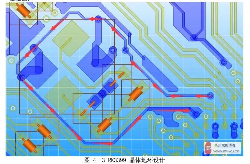
On the top layer beneath the crystal, a ground ring can be placed around it. The ground ring is connected to adjacent ground layers via vias to isolate noise;
-
Maintain a complete ground reference plane on the second layer beneath the crystal, avoiding any trace segmentation, which helps isolate noise and maintain the stability of the crystal output;
-
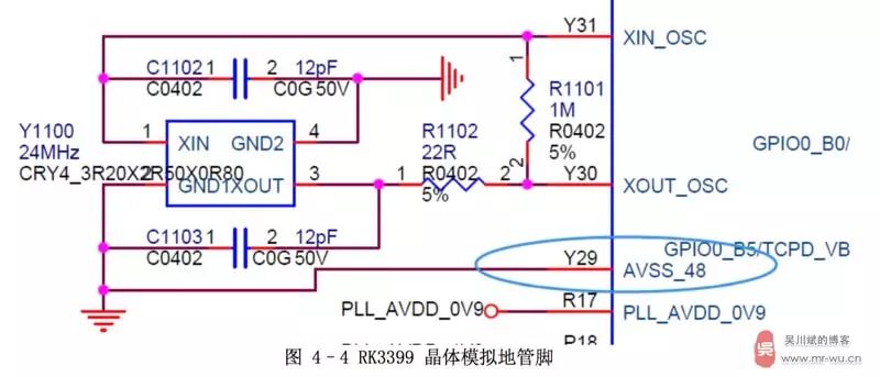
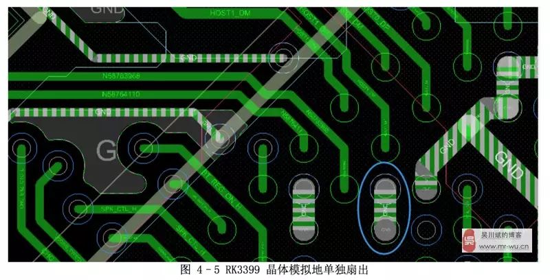
Y29 serves as the analog ground for the crystal. During layout, please ensure it is isolated from other digital grounds and connected separately to the ground reference plane on the second layer via vias;