Storage Principles of NAND Flash
The basic architecture of the smallest unit in solid-state drives is as follows:
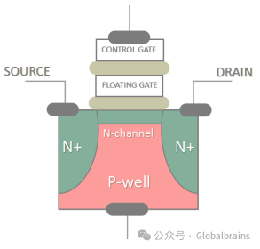
We know that all information storage in computers ultimately must return to 0 and 1. In principle, as long as the storage unit can provide two or more distinguishable states, it can be used to record data.
(1) Writing Data
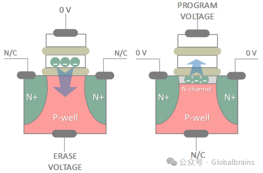
In NAND Flash, when we need to write data, we apply a high voltage to the control gate in the diagram, allowing electrons to flow from the source to the drain through the N-channel. Once the current is strong enough and the electrons gain sufficient energy, they will cross the silicon dioxide layer (SiO2) beneath the floating gate to be captured by the unit. This process is known as the Tunnel Effect;
(2) Data Stability
Once electrons enter the floating gate, even if the power is removed, as long as there is not enough energy, the electrons cannot escape from the silicon dioxide layer beneath, and the captured state of the electrons will be maintained for a long time, potentially lasting for decades, depending on the degradation of the insulating silicon dioxide layer.
(3) Reading Data
When reading data, we also apply voltage to the control gate to attract the electrons in the floating gate, but not as high as during tunnel injection. At the same time, we allow current to flow through the N-channel, using the current to sense the amount of electrons captured in the floating gate, converting the intensity of the signal into binary 0s and 1s, which are then output as data.
(4) Erasing Data
If we need to erase data, we must release the electrons in the floating gate. At this time, we do not apply any voltage to the control gate but instead apply voltage to the P-type semiconductor (P-Well) beneath the unit. When the current flows through the silicon dioxide layer beneath the N-channel, it reverses the flow, allowing the electrons in the floating gate to cross back through the silicon dioxide layer and be released. This process is called Tunnel Release.
Simple Analysis of SLC, MLC, and TLC
1. Introduction to SLC, MLC, and TLC
SLC (Single-Level Cell) means that each storage unit only stores 1 bit of information, relying on the presence or absence of electrons captured in the floating gate to output data (even in the 0 state, there are still some electrons in the floating gate, but not many), which is the simplest representation of 0 and 1;
MLC (Multi-Level Cell) means that each storage unit can store 2 bits of information, with the amount of electrons in the floating gate divided into four states: high, medium, low, and none, which translates to binary 00, 01, 10, and 11;
TLC (Triple-Level Cell) further divides the captured states of electrons in the floating gate into eight states, which translates to binary 000, 001, 010, 011, 100, 101, 110, and 111, representing 3 bits.
2. Comparison of SLC and MLC
The comparison between SLC and MLC can be divided into five aspects: lifespan, cost, power consumption, performance, and error rate.
(1) Lifespan Comparison
- Principle Explanation
Solid-state drives primarily store data based on the amount of electrons captured in the floating gate. Electrons must enter or leave the floating gate through the tunnel effect, crossing the silicon dioxide layer that blocks the electrons. The silicon dioxide layer is only about 10nm thick, and with each tunnel injection or release of electrons, the atomic bonds of the silicon dioxide are gradually damaged. Therefore, the data erasure process becomes slower over time, as electrons gradually occupy the insulating silicon dioxide layer, counteracting the voltage applied to the control gate, leading to the need for higher voltages to complete the operation, which can cause the oxide to break down faster. Once the entire silicon dioxide layer is penetrated by electrons, that unit is officially at the end of its life.
- Conclusion
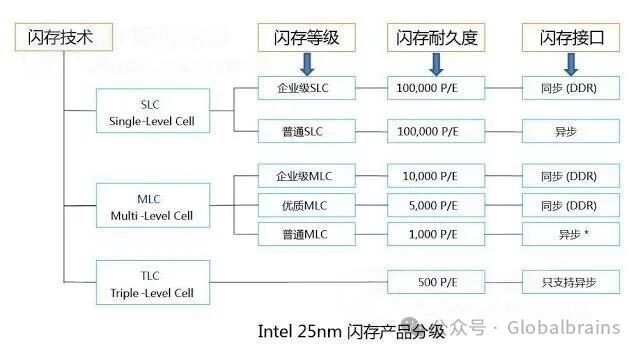
SLC has only two states (on or off), while MLC has four voltage states. To achieve these four states, electrons must frequently enter and exit the silicon dioxide layer, accelerating the depletion of the unit. This is why SLC can have a lifespan of up to 100,000 write cycles, while MLC only has about 10,000 cycles.
Of course, TLC is even worse, averaging only 500 to 1,000 write cycles, so it is mainly used for budget-friendly USB drives.
(2) Comparison of Speed, Power Consumption, Stability, Error Rate, and Cost
SLC, having only two states, is the easiest to identify, making it the fastest under the same controller chip and logic conditions, with the lowest power consumption and stable states. In modern technology, the error rate is almost negligible.
One SLC cell stores 1 bit of data, while one MLC cell can store 2 bits or more, but the chip size does not increase, effectively compressing the stored data. This results in a larger capacity for the same chip area, naturally lowering the price.
Both MLC and TLC heavily rely on ECC (Error Correction Code); any error can lead to multiple data losses. Fortunately, by the end of 2012, ECC technology from major manufacturers had matured significantly.
(3) Comparison of Storage Capacity
As of August 1, 2017, for single Flash chips, SLC supports a maximum of 512GB, MLC supports a maximum of 4TB, and TLC supports a maximum of 6TB.
Clarification on Memory Chip Grades
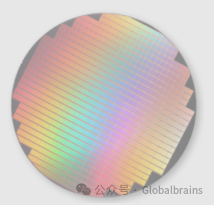
The image above shows what is known as a wafer, which looks like this right after being cut from the factory. Each small square can be made into a memory card. The issue is that, just like memory chips, not every piece on the wafer is of high quality. For companies like Intel and Micron (whose wafers are produced by the jointly owned IMFT, IM Flash Technology),
(1) Some can be used to make the highest grade synchronous chips;
(2) Some can be used as mid-grade synchronous chips after repair and verification;
(3) And some, no matter how they are processed, are subpar, not worth using, but can still be sold as low-grade asynchronous chips, mainly used in budget memory cards.
So, do not assume that just because it is branded Intel or Micron, it is of premium quality; it is not that simple, and you need to refer to the coding on the chip surface to determine the quality.
Synchronous vs. Asynchronous
The definition of synchronous/asynchronous chips mainly lies in the different definitions of two pins. In synchronous mode, the chip does not need to inform the controller “I am ready to read/write”; instead, it is always in a ready state, saving a clock cycle.
Using Intel’s 25nm chip grading table to summarize, here is a clear outline.