The SPI (Serial Peripheral Interface) communication protocol is a high-speed, full-duplex, synchronous, master-slave architecture serial communication protocol that uses only four signal lines. It is widely used for data transmission between MCUs/FPGA and peripherals (such as DACs, ADCs, Flash, and EEPROM).This article will explain the SPI communication protocol in three parts: the physical layer, protocol layer, and its applications.1 SPI Physical LayerThe connection methods between SPI communication devices can be divided into one master and one slave and one master and multiple slaves, with the latter further divided into two modes: independent mode and daisy chain mode.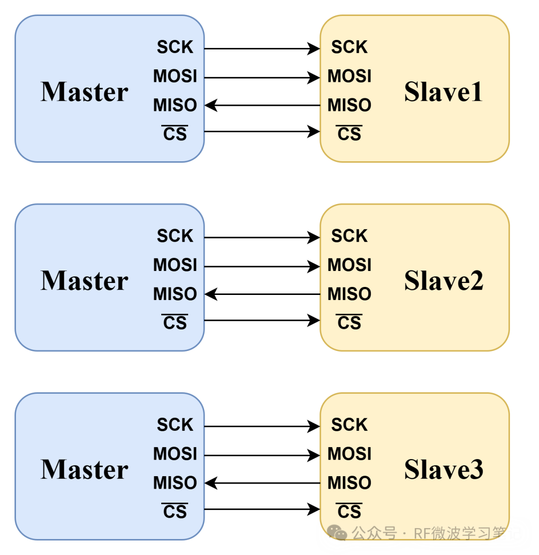 Figure 1: One Master One Slave SPI Communication Device Connection DiagramFigure 1 shows the one master one slave connection method, where the master device can exchange data with multiple slave devices simultaneously.
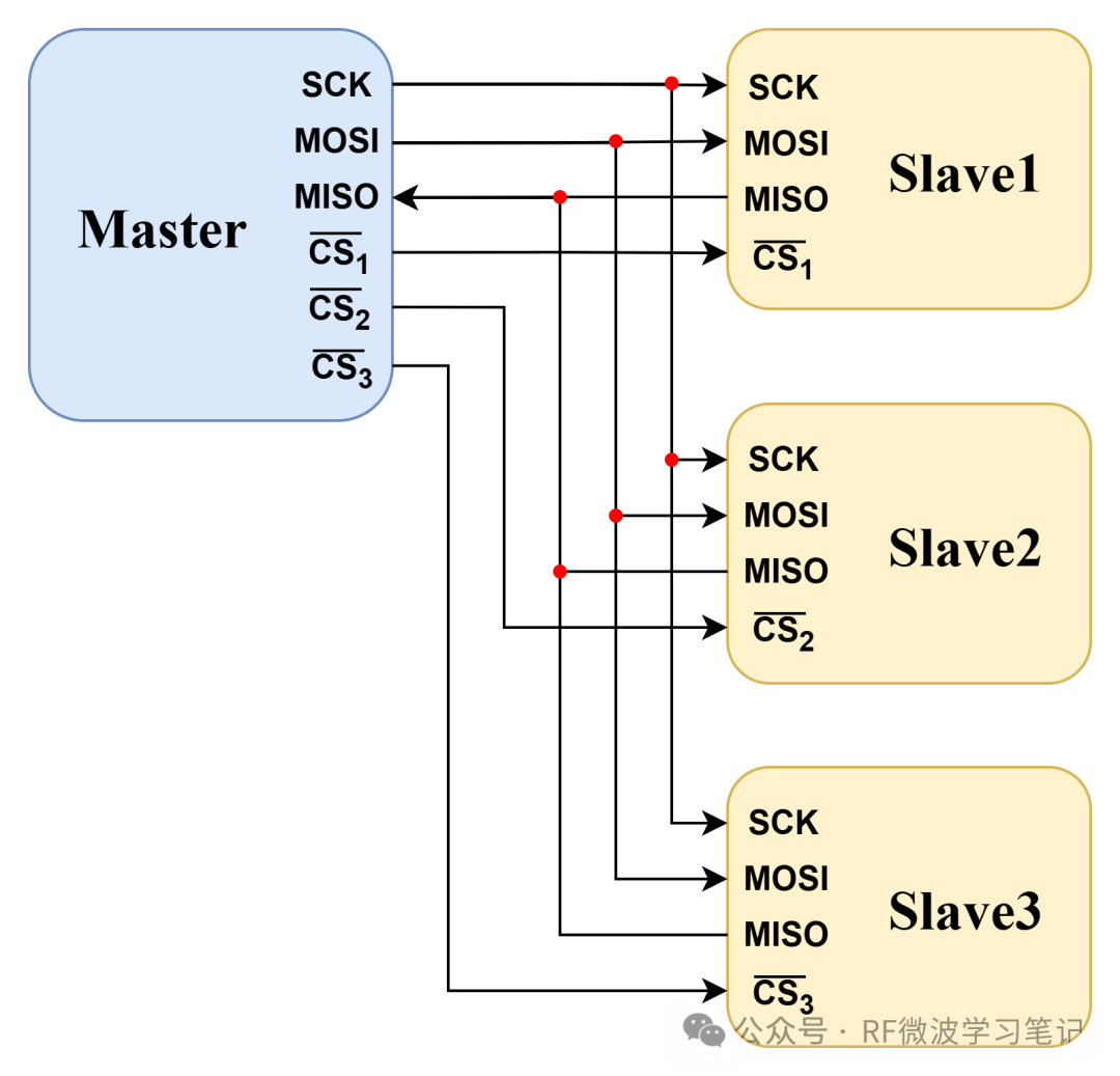 Figure 2: One Master Multiple Slaves Independent ModeIn the one master multiple slaves independent mode, the slave devices share the SCK, MOSI, and MISO lines, each having an independent CS line. The master device communicates with a specific slave device by pulling down a particular CS line.
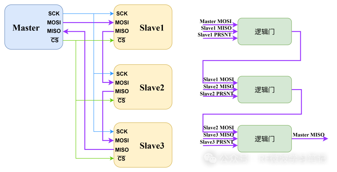 Figure 3: One Master Multiple Slaves Daisy Chain
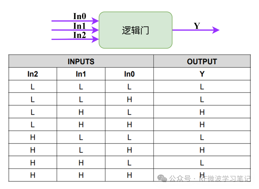 Figure 4: Logic Gate Truth TableIn the one master multiple slaves daisy chain mode, all slave devices share the SCK and CS lines, while MOSI and MISO are connected in series. When the logic gate Slave1 PRSNT is pulled low, while Slave2 PRSNT and Slave3 PRSNT remain high, the master device communicates with Slave1, and so on. The logic gate can be selected based on the application scenario.From the above, it can be seen that the one master one slave connection method can exchange data with multiple slave devices simultaneously, but requires 4n signal lines. The one master multiple slaves connection method can only communicate with one slave device at a time; for the independent mode, it requires 3+n signal lines, while the daisy chain mode only requires 4 signal lines.The SPI communication protocol includes one clock line SCK, two data lines MOSI (Master Output, Slave Input) and MISO (Master Input, Slave Output), and one chip select line CS (Chip Select). Their functions are summarized in the table below:Table 1: Functions of SPI Signal Lines
| Signal Line | Function |
| SCK | Clock signal line used to synchronize communication data. Generated by the master device, it determines the communication rate, which is limited by the lowest maximum clock frequency supported by the devices. |
| MOSI | Master device output/slave device input line, where the master outputs data from this signal line, and the slave reads the data sent by the master from this line, with data direction from master to slave. |
| MISO | Master device input/slave device output line. The master reads data from this signal line, and the slave outputs data to the master from this line, with data direction from slave to master. |
| CS | Chip select signal line used by the master device to select the slave device to communicate with, generated by the master device, active low. Thus, SPI communication starts with the CS line pulled low and ends with it pulled high. |
SPI pins generally use push-pull mode: they can actively output high (push) and low (pull), providing strong driving capability and good signal noise immunity.2 SPI Protocol LayerThe SPI communication protocol has four communication modes defined by clock polarity (CPOL) and clock phase (CPHA). The CPOL parameter specifies the level state of the SCK clock signal when idle (CS is high, device not selected), while CPHA specifies whether data sampling occurs on the odd or even edge of the SCK clock.Mode 0: CPOL=0, CPHA=0. When CS=1, SCK=0; data is sampled on the odd edge of SCK (rising edge); data is updated on the even edge of SCK (falling edge).Mode 1: CPOL=0, CPHA=1. When CS=1, SCK=0; data is sampled on the even edge of SCK (falling edge); data is updated on the even edge of SCK (rising edge).Mode 2: CPOL=1, CPHA=0. When CS=1, SCK=1; data is sampled on the odd edge of SCK (falling edge); data is updated on the even edge of SCK (rising edge).Mode 3: CPOL=1, CPHA=1. When CS=1, SCK=1; data is sampled on the even edge of SCK (rising edge); data is updated on the odd edge of SCK (falling edge).The four modes are summarized in the table below:
| SPI Mode | CPOL | CPHA | CS=1 SCK | Data Sampling | Data Updating |
| 0 | 0 | 0 | Low | Rising Edge | Falling Edge |
| 1 | 0 | 1 | Low | Falling Edge | Rising Edge |
| 2 | 1 | 0 | High | Falling Edge | Rising Edge |
| 3 | 1 | 1 | High | Rising Edge | Falling Edge |
Figure 5 shows the timing diagrams for the four SPI communication modes.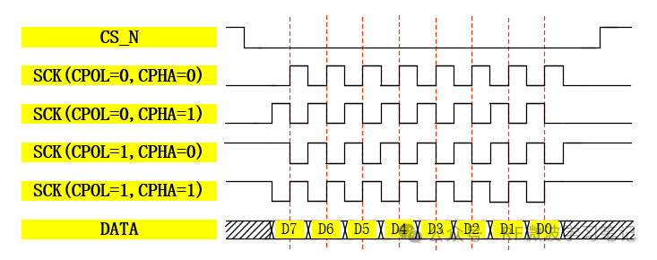 Figure 5: SPI Communication Mode Timing DiagramAmong the four communication modes, modes 0 and 3 are commonly used, with data sampling occurring on the rising edge.SPI communication has the following characteristics:1) MOSI and MISO transmit 1 bit of data during each SCK clock cycle, and both occur simultaneously (full-duplex).2) CS transitions from high to low, signaling the start of SPI communication; CS transitions from low to high, signaling the end of SPI communication.3) There is no strict requirement on whether SPI data transmission is MSB-first or LSB-first; generally, the MSB-first mode is used as shown in Figure 5.4) The basic unit of data transmission in SPI is a frame, which can be 8 bits or 16 bits, and there is no limit on the number of frames transmitted at a time.3 Application ExampleTaking the AD5664R DAC as an example, with a resolution of 16 bits and a clock frequency of 50 MHz. The functional block diagram is shown below, as a slave communicating with the master MCU (SPI protocol).SCLK is the clock pin SCK, SYNC is the chip select pin CS, and DIN is the slave input MOSI.
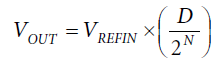
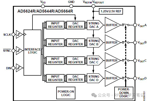 AD5664R has four outputs: VOUTA VOUTB VOUTC VOUTD; it has internal and external reference voltages. When selecting the internal reference voltage of 1.25V (AD5664R-3), the VREFIN/VREFOUT pin outputs the internal reference voltage. When selecting the external reference voltage, the VREFIN/VREFOUT pin is for external reference voltage input.When using the external reference voltage, the output voltage value of AD5664R-3 is:
 When using the internal reference voltage (1.25V), the output voltage value of AD5664R-3 is:
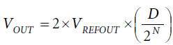 Where D is the decimal number loaded into the DAC REGISTER (AD5664R-3 16bit: 0~65535); N is the DAC resolution (AD5664R-3 16bit).INPUT REGISTER is a 24-bit shift register:
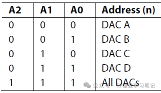
 Where the low 16 bits are data bits (DATA BITS), the truth table for COMMAND BITS and ADDRESS BITS is as follows:
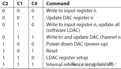 The common command is 011 (C2 C1 C0): write and update DAC channel
 Now, we will use the SPI communication protocol to write data into the DAC INPUT REGISTER, with the timing diagram shown below:
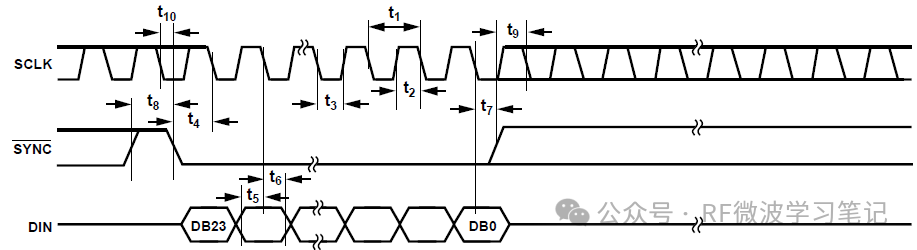 The timing in the timing diagram is as follows:
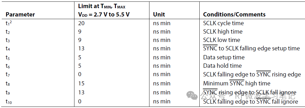 t1=20ns is the SCK clock cycle, corresponding to a clock frequency of 50MHz.From the timing diagram, it can be seen that: when CS=1, SCK=1, and sampling occurs on the falling edge, thus the SPI communication protocol used is mode 2.4 Referenceshttps://doc.embedfire.com/fpga/altera/ep4ce10_pro/zh/latest/code/spi_flash.html
https://www.mouser.cn/datasheet/3/1014/1/ad5624r_5644r_5664r.pdf