1. Data Communication Methods
1. Serial and Parallel Communication
According to the method of data transmission, communication can be divided into serial communication and parallel communication.
Serial Communication: This refers to the communication method where devices transmit data one bit at a time through a single data signal line, ground line, and control signal line. At the same time, only one bit (bit) of data can be transmitted.
Parallel Communication: This refers to the communication method that uses 8, 16, 32, or more data lines (the number of signal lines corresponds to the number of data bits) to transmit multiple data bits simultaneously.
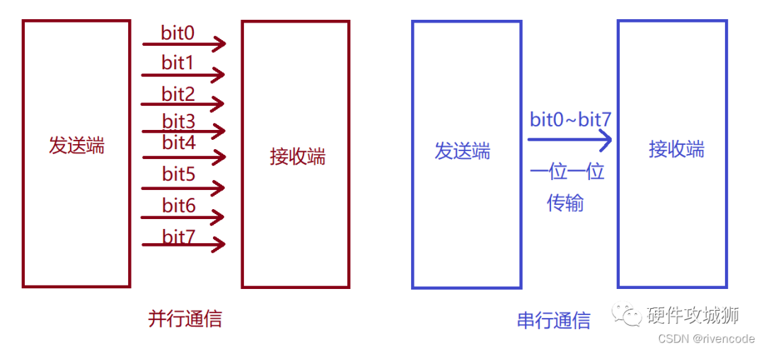
Comparison of Characteristics between Serial and Parallel Communication:

Parallel communication can send multiple bits of data simultaneously, so it is much faster than serial communication. However, parallel communication requires more data lines, making it relatively more expensive, and it has higher synchronization requirements. As the communication speed increases, signal interference can significantly affect communication performance.
2. Full Duplex, Half Duplex, and Simplex Communication
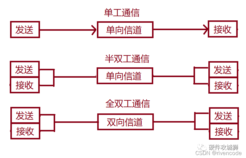
Simplex Communication: This is a communication method where information can only be transmitted in one direction. One device is fixed as the sender, and the other as the receiver. The sender can only send information and cannot receive it, while the receiver can only receive information and cannot send it. Only one signal line is needed.
Half Duplex Communication: This allows for bidirectional communication but cannot occur simultaneously in both directions. It must alternate, which can also be understood as a type of simplex communication that can switch directions. At the same time, only one direction can transmit data, requiring only one data line.
Full Duplex Communication: This allows both devices to send and receive data simultaneously at the same time. Full duplex does not require direction switching, and both parties need to have both a transmitter and a receiver, requiring 2 data lines.
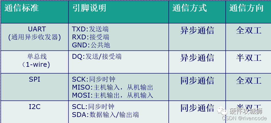
Common Serial Communication Interfaces:
3. Synchronous and Asynchronous Communication
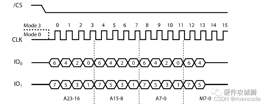
Synchronous Communication: Both sending and receiving devices use a signal line to indicate the clock signal, coordinating and synchronizing data under the drive of the clock signal. In communication, it is often specified that data sampling occurs on the rising or falling edge of the clock signal, corresponding to clock polarity and clock phase.
SPI Synchronous Communication:
Asynchronous Communication: This does not require a clock signal for data synchronization. Instead, it intersperses some synchronization signal bits directly within the data signal or packages the main data into a data frame (for serial ports: start bit, data, optional parity bit, stop bit) format. In some communications, both parties need to agree on the transmission rate (baud rate) for better synchronization.

2. Serial Communication Protocol
Communication Protocol: Divided into physical layer and protocol layer. The physical layer specifies the characteristics of the mechanical and electronic functional parts of the communication system, ensuring the transmission of raw data over physical media (to put it simply, the hardware part). The protocol layer mainly specifies the communication logic, unifying the data packaging and unpacking standards for both sending and receiving parties (software).
STM32 Serial Overview
USART – Universal Synchronous Asynchronous Receiver and Transmitter is a serial communication device that can flexibly perform full-duplex data exchange with external devices. Unlike USART, there is also UART (Universal Asynchronous Receiver and Transmitter), which is a simplified version of USART that removes the synchronous communication function (clock synchronization) and only supports asynchronous communication. A simple distinction between synchronous and asynchronous is whether a clock output needs to be provided externally during communication. The serial communication we commonly use is basically UART.
Serial communication generally transmits data in frame format, meaning data is transmitted frame by frame, with each frame containing a start signal, data information, parity information (set by us), and a stop signal.
1. Physical Layer
1) RS232 Standard
Many microcontrollers, such as those we use with STM32, as well as some sensors, generally operate at TTL levels.
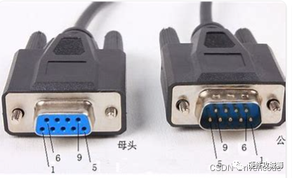
RS232 is a form of serial data transmission known as serial connection, with the classic sign being the 9-pin DB9 cable. RS232 voltage represents logic 1 and 0, greatly enhancing fault tolerance, mainly used for direct communication between industrial equipment.
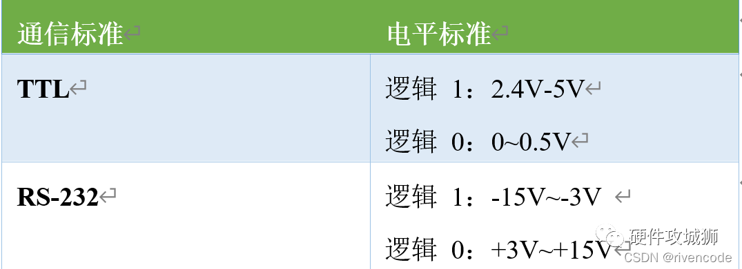
As can be seen from the above figure, TTL and RS-232 standards are logically opposite, and the levels are quite different. If a microcontroller communicates with another microcontroller or other TTL devices using RS-232 communication (DB9), a level conversion from TTL to RS232 and RS232 to TTL must be performed.

Two communication devices establish a connection between their “DB9 interfaces” via serial signal lines, using the “RS-232 standard” to transmit data signals. Since RS-232 level standard signals cannot be directly recognized by the controller, these signals pass through a “level conversion chip” to convert them into “TTL standard” level signals that the controller can recognize, enabling communication.
DB9 Serial Line:
2) USB to Serial (Key Point)
The reason this is a key point is that this is the method I use for experiments, so I will focus on it:
USB to Serial: Mainly used for communication between devices (STM32) and computers.

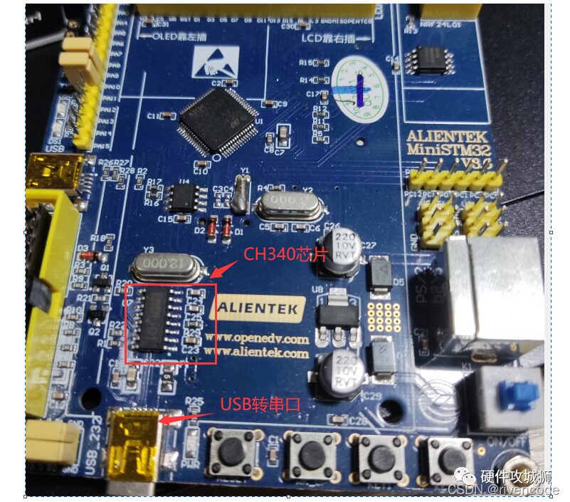
Level conversion chips generally include CH340, PL2303, CP2102, FT232.
When using these, the computer must install the driver for the level conversion chip (to create a virtual serial port). Here I have installed CH340.
Principle Diagram: It is essential to understand the following diagram.
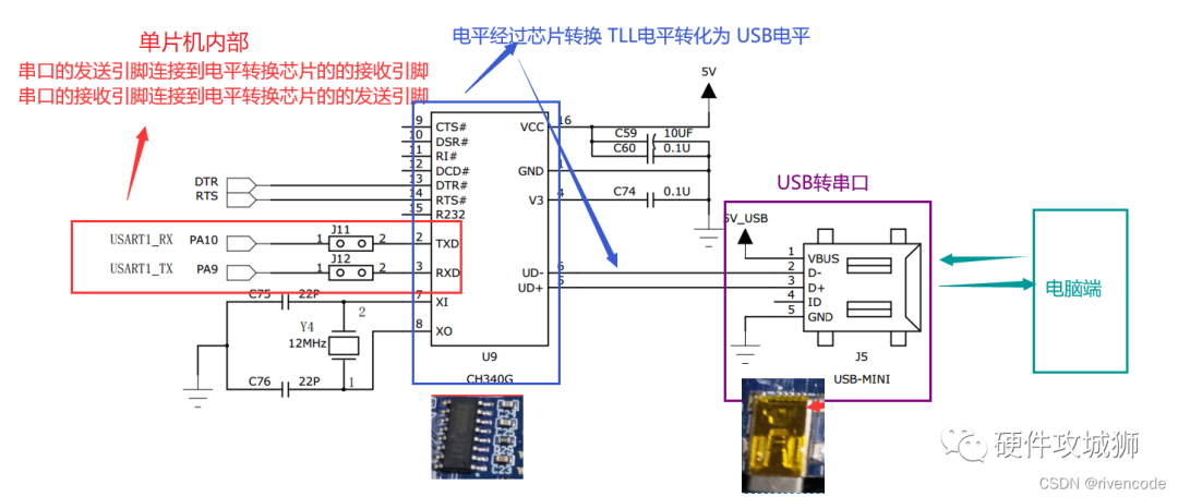
This is a schematic from a Wildfire project, as I believe the Atom’s diagram is poorly drawn, but the principles are consistent.
3. Native Serial to Serial

Native serial communication mainly refers to communication between the controller and serial devices or sensors that use TTL levels, without needing a level conversion chip, directly using TTL level communication, such as GPS modules, GSM modules, serial to WIFI modules, and HC04 Bluetooth modules.
2. Protocol Layer
The protocol layer of serial communication specifies the content of the data packet, which consists of a start bit, main data, a parity bit, and a stop bit. Both parties in the communication must agree on the data packet format (the same start bit, data, parity bit, and stop bit) to successfully send and receive data.

1) Start and Stop Signals of Communication
A data packet in serial communication starts with a start signal and ends with a stop signal. The start signal of the data packet is represented by a logic 0 bit, while the stop signal can be represented by 0.5, 1, 1.5, or 2 logic 1 bits.
1 stop bit: This is the default value for the number of stop bits.
2 stop bits: Can be used for standard USART mode, single-wire mode, and modem mode.
0.5 stop bits: Used when receiving data in smart card mode.
1.5 stop bits: Used when sending and receiving data in smart card mode.
2) Valid Data
Immediately following the start bit in the data packet is the main data content to be transmitted, also known as valid data. The length of valid data is usually agreed upon to be 5, 6, 7, or 8 bits long.
3) Data Parity
Even Parity: The parity bit ensures that the number of ‘1’s among the 7 or 8 LSB data bits and the parity bit is even.
For example: Data = 00110101, which has 4 ‘1’s. If even parity is chosen (PS = 0 in USART_CR1), the parity bit will be ‘0’. The final data check will confirm that if there is an even number of ‘1’s, then the data transmission is error-free (but this is not absolute; if two bits are sent incorrectly (0 becomes 1), then it will still be even).
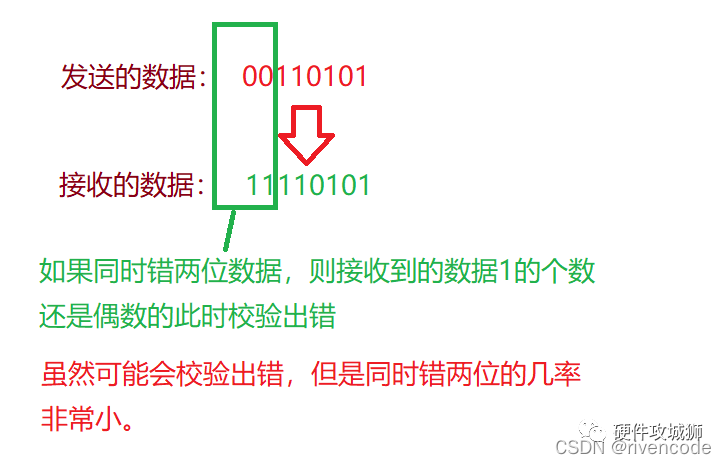
Odd Parity: This parity bit ensures that the number of ‘1’s among the 7 or 8 LSB data bits and the parity bit is odd.
For example: Data = 00110101, which has 4 ‘1’s. If odd parity is chosen (PS = 1 in USART_CR1), the parity bit will be ‘1’. The final data check will confirm that if there is an odd number of ‘1’s, then the data transmission is error-free, but again, this is not absolute (if two ‘1’s become ‘0’s).

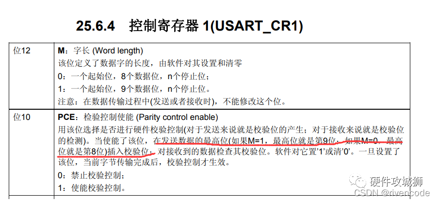
Transmission Mode: If the PE bit in USART_CR1 is set, and if odd/even parity fails, the PE flag in the USART_SR register is set to ‘1’, and if the PEIE bit in the USART_CR1 register is pre-set, an interrupt is generated (we can write code to handle parity failures in the corresponding interrupt service function).


3. USART Functional Block Diagram (Super Important)
Understanding the functional block diagram thoroughly will make writing code a breeze. It is absolutely essential to master!!!

1. Functional Pins:
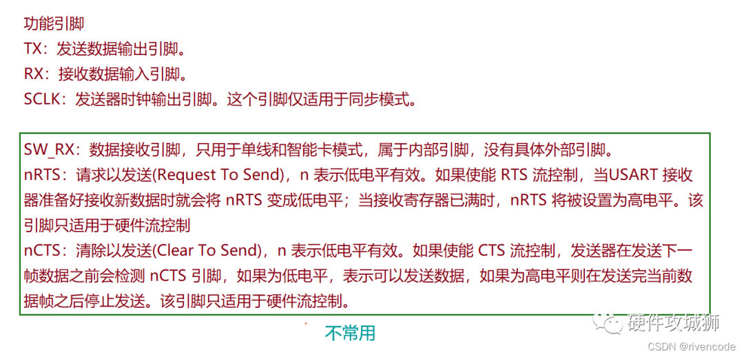
2. Data Register (Key Point)

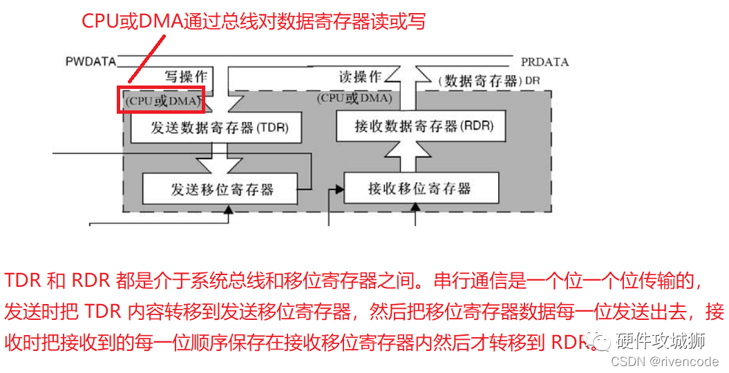
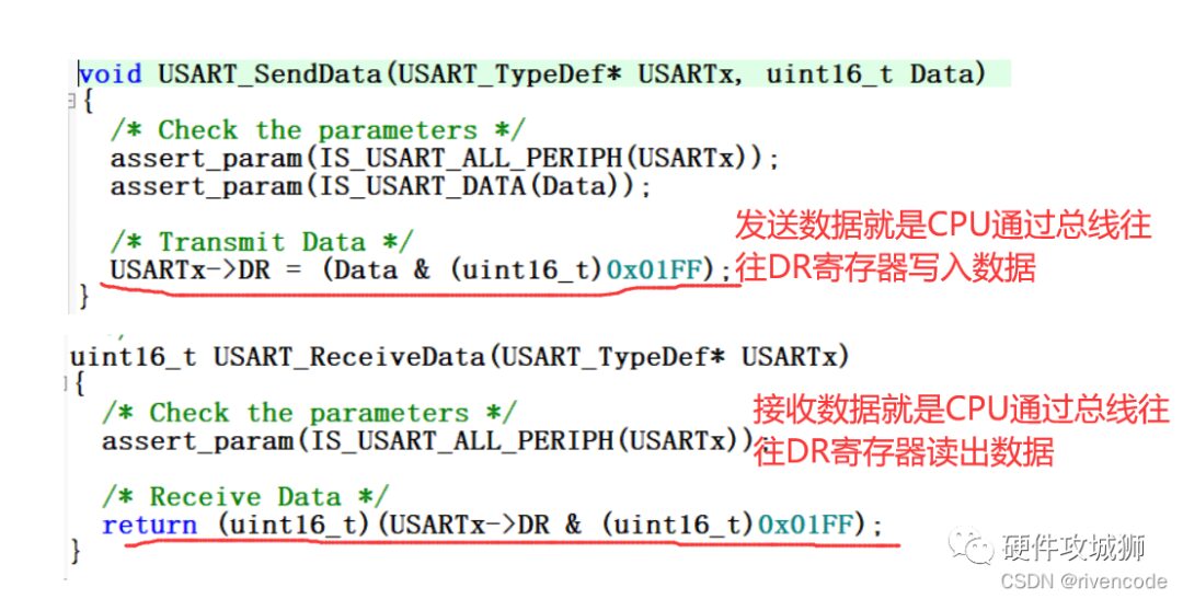
Understanding the following diagram is also very important!!
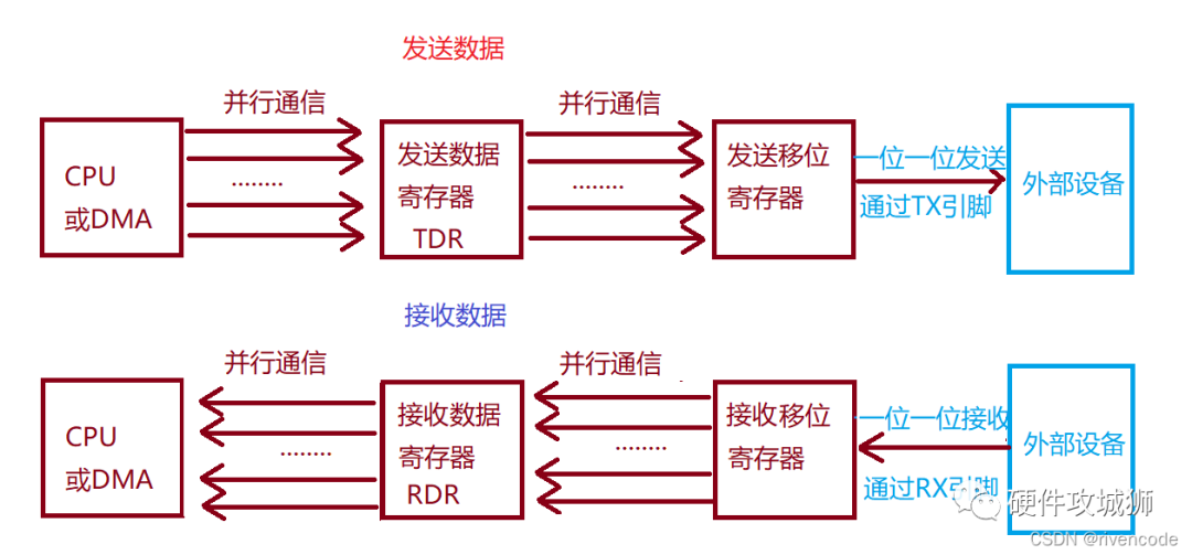
3. Control Unit (Key Point)
Transmitter
The transmitter sends 8 or 9 bits of data based on the status of the M bit. When the transmit enable bit (TE) is set, the data in the send shift register is output on the TX pin, and the corresponding clock pulse is output on the CK pin.
A character frame transmission requires three parts: start bit + data frame (which may include parity bit) + stop bit. Each character (a data frame) begins with a low-level start bit, followed by a configurable number of stop bits, and the data frame is the 8 or 9 bits of data we want to send, transmitted starting from the least significant bit. The stop bit is a high level of a certain time period.
Configuration Steps:
1. Activate USART by setting the UE bit in the USART_CR1 register.

2. Set the M bit in USART_CR1 to define the word length.

3. Configure the number of stop bits in USART_CR2.

4. If using multi-buffer communication, configure the DMA enable bit (DMAT) in USART_CR3. Configure the DMA register as described in multi-buffer communication; more on DMA will be explained in detail next time.

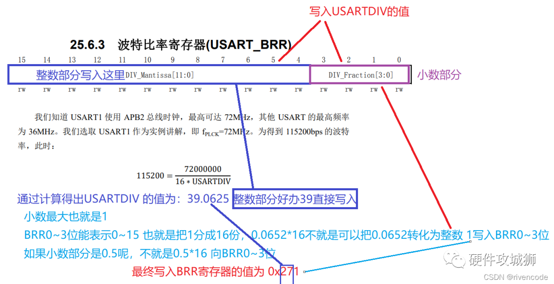
5. Use the USART_BRR register to select the required baud rate.
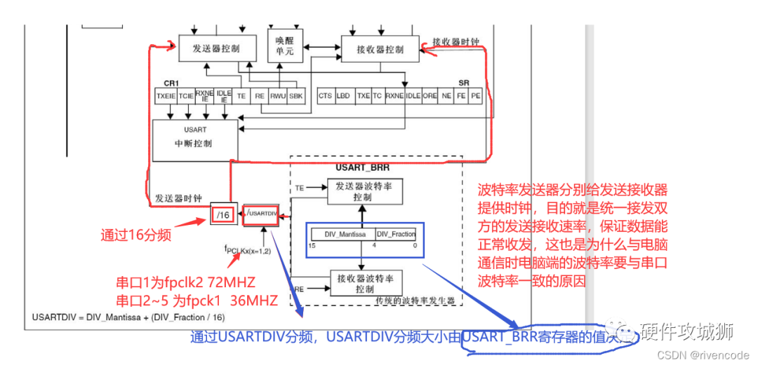
Sending and receiving are driven by a shared baud rate generator. When the transmitter and receiver enable bits are set, it generates the clock for each.

Here’s an example: at a baud rate of 115200.
6. Set the TE bit in USART_CR1 and send an idle frame (a high level of one data frame length) as the first data transmission.

7. Write the data to be sent into the USART_DR register (this action clears the TXE bit). In the case of having only one buffer, repeat step 7 for each data to be sent.

8. After writing the last data word into the USART_DR register, wait for TC=1, indicating that the transmission of the last data frame has ended (all data in the shift register has been sent). Before closing USART or entering sleep mode, it is necessary to confirm the end of transmission to avoid disrupting the last transmission.

Understanding the TXE and TC bits deeply:
Clearing the TXE bit is always accomplished by writing to the data register (CPU or DMA). When the TXE bit has been set to 1 by hardware, it indicates:
● Data has been transferred from TDR to the shift register, and data transmission has begun (the data in the shift register is being transmitted bit by bit).
● The TDR register has been cleared.
● The next data can be written into the USART_DR register without overwriting the previous data. If the TXEIE bit is set, this flag will generate an interrupt.
If the USART is currently sending data (the data in the shift register is being transmitted bit by bit), writing to the USART_DR register will store the data in the TDR register, and when the current transmission ends, this data will be copied into the shift register, meaning that the data in the shift register will not be overwritten. Therefore, I believe that as long as you send a frame of data and wait for TXE to be set to 1, there is no need to wait for TC=1, even when sending multiple frames of data.
If the USART is idle and not sending data, writing to the USART_DR register will directly place the data into the shift register, and data transmission will begin, immediately setting the TXE bit.
When a frame has been completed (after the stop bit has been sent) and the TXE bit has been set, the TC bit will be set. If the TCIE bit in the USART_CR1 register has been set, an interrupt will be generated.
Use the following software process to clear the TC bit:
1. Read the USART_SR register once;
2. Write to the USART_DR register once.
The TC bit can also be cleared by writing ‘0’ to it. This clearing method is only recommended for use in multi-buffer communication mode.
Receiver
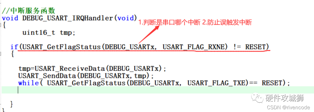
If the RE bit in the USART_CR1 register is set to 1, it enables USART reception, allowing the receiver to start searching for the start bit on the RX line. Once the start bit is detected, the data is stored in the receive shift register based on the RX line level state. After receiving is complete, the data from the receive shift register is moved to the RDR, and the RXNE bit in the USART_SR register is set to 1. If the RXNEIE bit in the USART_CR2 register is set to 1, an interrupt can be generated.
When a character is received:
● The RXNE bit is set to 1, indicating that the contents of the shift register have been moved to the RDR. In other words, the data has been received and can be read out.
● If the RXNEIE bit is set, an interrupt is generated.
● In multi-buffer communication, the RXNE bit is set after each byte is received and cleared by the DMA read operation on the data register.
● In single buffer mode, the RXNE bit is cleared through software by reading the USART_DR register. The RXNE flag can also be cleared by writing ‘0’ to it. The RXNE bit must be cleared before the next character is received (when the receive shift register is full) to avoid overflow errors (the data in the shift register will be overwritten).
Overflow Error
If the RXNE has not been reset (the data in the DR register has not been read out), and another character is received, an overflow error occurs. Data can only be transferred from the shift register to the RDR register after the RXNE bit has been cleared. The RXNE flag is set after each byte is received. If the next data has been received or the previous DMA request has not been serviced, the RXNE flag remains 1, resulting in an overflow error.
When an overflow error occurs:
● The ORE bit is set.
● The contents of the RDR will not be lost. Reading the USART_DR register will still get the previous data.
● The previous contents in the shift register will be overwritten. Any subsequently received data will be lost.
● If the RXNEIE bit is set or the EIE and DMAR bits are set, an interrupt is generated.
● Sequentially reading the USART_SR and USART_DR registers can reset the ORE bit.

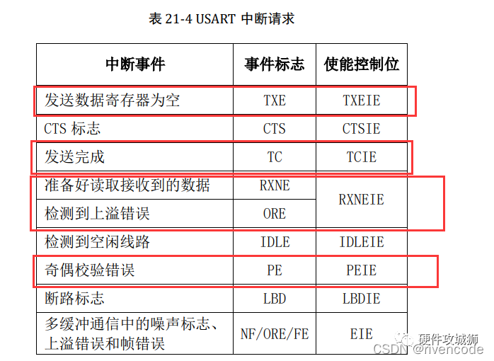
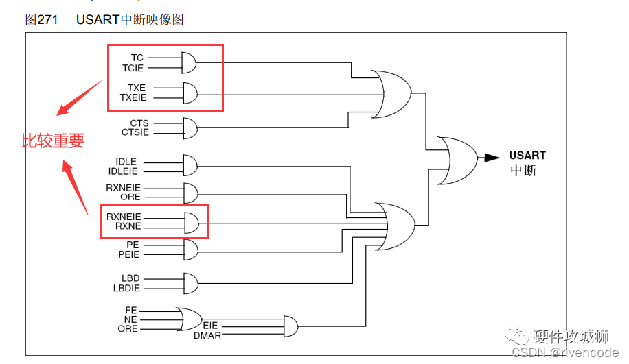
USART Related Interrupts:

4. USART Initialization Structure
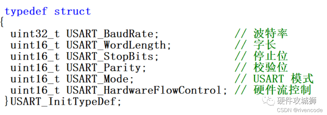
The members of the structure above that need to be configured for which register and which bit have been basically discussed earlier, so they will not be repeated here.
1) USART_BaudRate: Baud rate setting. Generally set to 2400, 9600, 19200, 115200. The standard library function will calculate the USARTDIV value and write it to the USART_BRR register.
2) USART_WordLength: Data frame word length, can be 8 or 9 bits. This sets the value of the M bit in the USART_CR1 register. If no parity bit is enabled, 8 data bits are generally used; if parity is enabled, 9 data bits are generally set, with the last bit being the parity bit.
3) USART_StopBits: Stop bit setting, can be 0.5, 1, 1.5, or 2 stop bits, which sets the STOP bits in USART_CR2. Generally, we choose 1 stop bit.
4) USART_Parity: Parity control selection, values for the PCE and PS bits in the USART_CR1 register.
5) USART_Mode: USART mode selection, allowing logical OR operations to select both USART_Mode_Rx and USART_Mode_Tx, corresponding to the RE and TE bits in the USART_CR1 register.
6) USART_HardwareFlowControl: Hardware flow control selection, which is only valid in hardware flow control mode, can choose to enable RTS, enable CTS, enable both RTS and CTS, or not enable hardware flow control.
5. USART1 Transmission and Reception Experiment
usart.h
usart.c
main.c
Regarding the printf function and scanf function redirection issue
MicroLib is an alternative library to the default C library that can fit into a small amount of memory and is used in conjunction with embedded applications that do not run in an operating system.

If you want to use the printf function to output data to the serial port, the printf function defaults to output to the screen (standard output stream—stdout), so you need to redirect the output stream to USART1 serial port 1.
When using the printf function, it will automatically call the fputc function, and the fputc function will redefine the output device to STM32’s USART1, so the output data will appear on serial port 1.

The scanf function (default keyboard input, we want to redirect it to serial reception) is similar, so I won’t elaborate.
Experimental Results


5. Sending Instructions to the Microcontroller to Light Up the LED
main.c
Copyright Statement: This article is an original piece by CSDN blogger “rivencode”, following the CC 4.0 BY-SA copyright agreement. Please include the original source link and this statement when reprinting.Original link:https://blog.csdn.net/k666499436/article/details/124354165


“Let’s Learn a Bit,” How Was Lei Jun’s Code from Over 30 Years Ago?
220V AC Zero-Cross Detection Circuit Design