When learning STM32 development, the debugging step is essential。This article will guide you through the knowledge related to debugging.
This article takes STM32F1 and Cortex-M3 as examples; the principles are the same or similar for other series chips or cores.
1Overview
In STM32, there are many debugging components. Using them, various debugging functions can be executed, including breakpoints, data watchpoints, flash address reloads, and various tracing.
STM32F1 uses the Cortex™-M3 core, which includes a hardware debugging module that supports complex debugging operations.
The hardware debugging module allows the core to halt when fetching instructions (instruction breakpoints) or accessing data (data breakpoints). When the core halts, both the internal state of the core and the external state of the system can be queried. After the query is completed, the core and peripherals can be restored, and the program will continue execution.
When the STM32F10x microcontroller is connected to a debugger and debugging begins, the debugger will use the core’s hardware debugging module for debugging operations.
2
Debugging Block Diagram
The debugging block diagram of STM32F1 and Cortex™-M3:
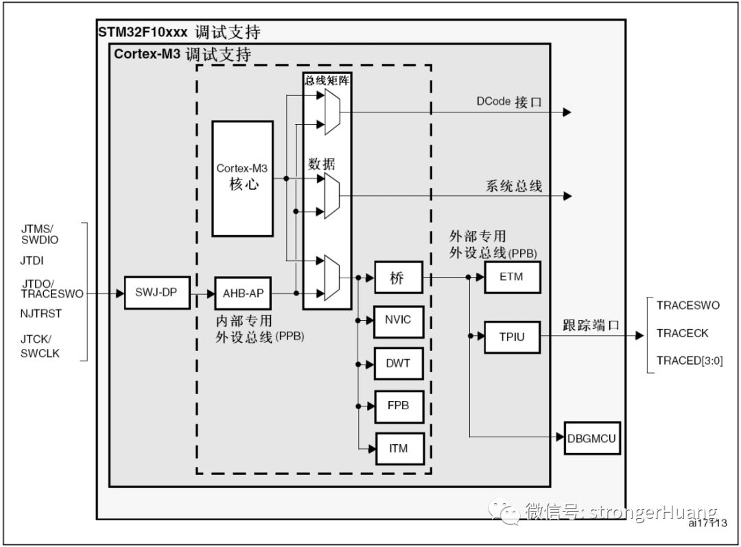
Note: The hardware debugging module contained in the Cortex™-M3 core is a subset of the ARM CoreSight development toolset.
The ARM Cortex™-M3 core provides integrated on-chip debugging capabilities. It consists of the following parts:
-
SWJ-DP: Serial/JTAG debug port
-
AHP-AP: AHB access port
-
ITM: Instrumentation Trace Macrocell
-
FPB: Flash Patch and Breakpoint Unit
-
DWT: Data Watchpoint and Trace
-
TPUI: Trace Port Interface Unit (only supported on larger package chips)
-
ETM: Embedded Trace Macrocell (only supported on larger packages with dedicated pins for STM32F1 debugging features)
-
Flexible debugging pin assignment
-
MCU debug box (supports low power modes, controls peripheral clocks, etc.)
3
Debugging Interfaces
STM32 supports two debugging interfaces:
-
Serial interface
-
JTAG debug interface
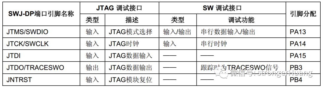
Five general I/O pins of STM32 can be used as SWJ-DP (Serial/JTAG debug) interface pins:
4
SWJ Debug Port (Serial Wire and JTAG)
The STM32 core integrates a Serial/JTAG debug interface (SWJ-DP). This is the standard ARM CoreSight debug interface, including the JTAG-DP interface (5 pins) and SW-DP interface (2 pins).
1. JTAG debug interface (JTAG-DP) provides a 5-pin standard JTAG interface for the AHP-AP module.
2. Serial debug interface (SW-DP) provides a 2-pin (clock + data) interface for the AHP-AP module.
In the SWJ-DP interface, the 2 pins of the SW-DP interface and some of the 5 pins of the JTAG interface are multiplexed.
SWJ Debug Port:
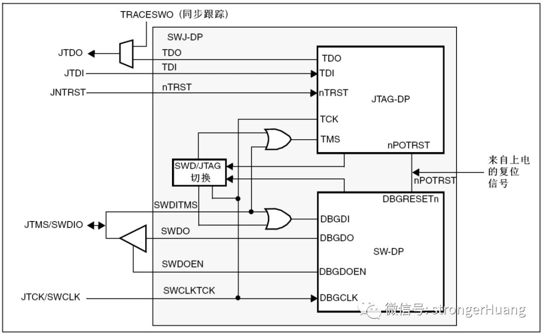
The above diagram shows that the asynchronous trace output pin (TRACESWO) and TDO are multiplexed. Therefore, the asynchronous tracing function can only be implemented on the SWDP debug interface and cannot be implemented on the JTAG-DP debug interface.
Switching Mechanism Between JTAG-DP and SW-DP
The JTAG debug interface is the default debug interface. If the debugger wants to switch to SW-DP, it must output a specific JTAG sequence on TMS/TCK (mapped to SWDIO and SWCLK, respectively) to disable JTAG-DP and activate SW-DP. This method can activate the SW-DP interface using only the SWCLK and SWDIO pins.
The specific sequence is:
1. Output TMS (SWDIO) = 1 signal for more than 50 TCK cycles
2. Output 16 TMS (SWDIO) signals 0111100111100111 (MSB)
3. Output TMS (SWDIO) = 1 signal for more than 50 TCK cycles
5
Internal Pull-up and Pull-down on JTAG Pins
It is crucial to ensure that the JTAG input pins are not floating, as they are directly connected to D flip-flops controlling the debugging mode. Special attention must be paid to the SWCLK/TCK pins, as they are directly connected to the clock terminals of some D flip-flops.
To avoid any uncontrolled I/O levels, STM32 embeds internal pull-up and pull-down resistors on the JTAG input pins.
-
JINTRST: Internal pull-up
-
JTDI: Internal pull-up
-
JTMS/SWDIO: Internal pull-up
-
TCK/SWCLK: Internal pull-down
Once the JTAG I/O is released by user code, the GPIO controller regains control. The states of these I/O pins will revert to their reset states.
-
JNTRST: Input with pull-up
-
JTDI: Input with pull-up
-
JTMS/SWDIO: Input with pull-up
-
JICK/SWCLK: Input with pull-down
-
JTDO: Floating input
Software can use these I/O pins as ordinary I/O pins.
6
Using Serial Interface and Releasing Unused Debug Pins as General I/O Pins
To utilize the serial debug interface and free up some general I/O pins, the user software must set SWJ_CFG=010 after reset, thus releasing PA15, PB3, and PB4 for use as general I/O pins.
During debugging, the debugger performs the following actions:
-
At system reset, all SWJ pins are assigned as dedicated pins (JTAG-DP + SW-DP).
-
In the system reset state, the debugger sends a specific JTAG sequence to switch from JTAG-DP to SW-DP.
-
Still in the system reset state, the debugger sets a breakpoint at the reset address
-
Releases the reset signal, and the core halts at the reset address.
-
From here, all debugging communication will use the SW-DP interface, and other JTAG pins can be repurposed by user code as general I/O pins.
Note: This is where everyone needs to configure the relevant pins.
7
References
1.Cortex™-M3 (r1p1 version) Technical Reference Manual (TRM)
2.ARM Debug Interface V5
3.ARM CoreSight Development Toolset (r1p0 version) Technical Reference Manual
Note: This article refers to the “STM32F1 Reference Manual” and “CM3 Technical Manual”.
Author: strongerHuang, Source: strongerHuang
Disclaimer: This article is reproduced with permission from the “strongerHuang” public account. The reproductionis for learning reference only and does not represent the views of this account. This account is not responsible for any infringement of its content, text, or images.
♥Click 👇 the business card to follow me♥
Previous Recommendations ·
1、The Most Comprehensive LED Lighting Program!
2、Sharing a Bug Location Method You Might Not Know
3、From Scratch, A Step-by-Step Guide to Writing a Serial Debug Assistant