Crystal Structure
Crystals can be divided into single crystals and polycrystals. If the atoms in the entire material are arranged in a regular and periodic manner, with a single structure throughout, it is called a single crystal, such as quartz single crystals, silicon single crystals, and rock salt single crystals. Polycrystals are made up of a large number of small single crystals randomly stacked together. Most actual crystals are polycrystalline, such as various metals and electronic ceramic materials. Due to the different relative orientations of the grains in polycrystals, their macroscopic properties often exhibit isotropy, and their shapes are irregular.
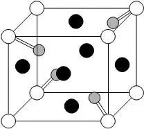
Semiconductor materials such as silicon and germanium belong to the diamond structure. The diamond structure can be seen as a face-centered cubic unit cell staggered by one-quarter the diagonal length along the body diagonal.
Crystal Planes and Directions
Crystals have the characteristic of anisotropy. When studying the physical characteristics of crystals, it is usually necessary to specify the orientation of the plane or the direction along which the crystal is oriented. For this reason, the concepts of crystal planes and crystal directions are introduced. To facilitate the determination and distinction of different orientations of crystal directions and planes, the Miller indices are commonly used internationally to standardize the indices for crystal directions and planes.
Crystal Direction Indices
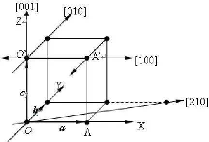
Taking a certain lattice point O of the unit cell as the origin, set the coordinate axes X, Y, Z through the origin O, using the length of the lattice vector as the unit of length for the axes; draw a straight line parallel to the desired crystal direction through the origin O, and select the nearest lattice point from the origin O on this line to determine the three coordinate values of this point; convert these three coordinate values into the smallest integers u, v, w, and enclose them in square brackets. [u v w] is the crystal direction index for the desired direction.
The crystal direction index represents all mutually parallel and directionally consistent crystal directions.
Crystal Plane Indices
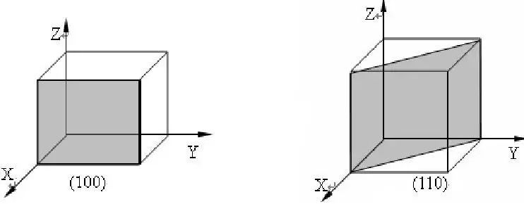
In the lattice, set a reference coordinate system, using the same method as when determining the crystal direction indices; select a crystal plane from the family of planes that does not pass through the origin, and determine the intercepts of this plane on each coordinate axis; take the reciprocals of each intercept; convert the three reciprocals into coprime integers and enclose them in parentheses, which represents the indices of that crystal plane, denoted as (h k l).
When the intercept of a crystal plane on one coordinate axis is negative, a “-” sign is added to the corresponding index. When the crystal plane is parallel to a certain coordinate axis, the intercept of the plane on that axis is considered to be ∞, and its reciprocal is 0.
The crystal plane indices represent not only a single crystal plane but also all mutually parallel crystal planes.
Defects in Crystals
Defects can be classified into point defects, line defects, plane defects, and bulk defects based on their geometric configuration in space.
01
Point Defects
Point defects are areas where the lattice structure deviates from strict periodicity, centered around vacancies, interstitial atoms, and impurity atoms within a microscopic region of one or several lattice constants.
02
Line Defects
Line defects are one-dimensional defects that deviate from the periodic lattice structure within the crystal. The most important type of line defect in crystals is dislocation.
03
Plane Defects and Bulk Defects
For crystals, there are also plane defects (stacking faults) and bulk defects (inclusions). Defects caused by disordered stacking sequences are called stacking faults, or simply faults. A fault is a regional defect, where atoms outside the fault are regularly arranged, and it is a type of plane defect. When the concentration of impurities added to the crystal exceeds the solubility limit, the impurities will precipitate within the crystal, forming bulk defects.
Impurities in Crystals
Practice shows that even trace amounts of impurities and defects can have a decisive impact on the physical and chemical properties of semiconductor materials.
Donor Impurities
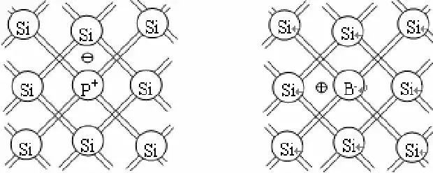
When phosphorus is doped into silicon, the phosphorus atoms occupy the positions of silicon atoms, resulting in the formation of a positively charged center and an extra valence electron. This type of impurity is called a donor impurity or n-type impurity.
Acceptor Impurities
When boron is doped into silicon, the boron atoms occupy the positions of silicon atoms, resulting in the formation of a negatively charged center and an extra vacancy. This type of impurity is called an acceptor impurity or p-type impurity.
Nowadays, 300mm wafer technology has matured, but as the diameter increases, the manufacturing difficulty also increases.
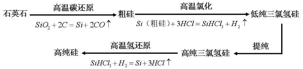
Growing Single Crystal Silicon
The main methods for preparing single crystal silicon are the Czochralski method (CZ method) and the floating zone melting method, with over 85% of single crystal silicon grown using the CZ method.
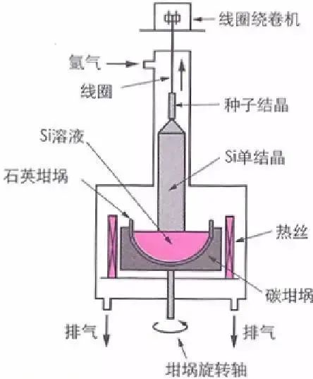
Single Crystal Furnace
A single crystal furnace can be divided into four parts: the furnace body, mechanical transmission system, heating temperature control system, and gas delivery system. The furnace body includes the furnace chamber, seed crystal shaft, quartz crucible, doping spoon, seed crystal cover, and observation window. The furnace chamber ensures uniform temperature distribution and good heat dissipation; the role of the seed crystal shaft is to drive the seed crystal to move up and down and rotate; the doping spoon contains the impurities to be doped; the seed crystal cover is to protect the seed crystal from contamination.
The mechanical transmission system mainly controls the movement of the seed crystal and crucible. To ensure that the Si solution is not oxidized, the vacuum requirement inside the furnace is very high, generally above 5 Torr, and the purity of the inert gas added must be above 99.9999%.
Growth Process
(1) Preparation
The purity of polycrystalline silicon must be very high, and it should be polished with hydrofluoric acid for cleaning purposes; defects on the seed crystal will be “inherited” by the newly grown crystal, so care must be taken to avoid defects when selecting the seed crystal; the crystal direction of the seed crystal must be the same as that of the crystal to be grown; the seed crystal must be cleaned; select the impurities to be doped based on the conductivity type of the crystal to be grown; clean the impurities; all cleaned materials should be rinsed with high-purity deionized water until neutral and then dried for later use. (2) Loading the Furnace The crushed polycrystalline silicon is loaded into the quartz crucible; the seed crystal is clamped onto the seed crystal shaft’s chuck, and the seed crystal cover is placed on top; the furnace is evacuated to a vacuum and filled with inert gas; check whether the leakage rate of the furnace body is acceptable. (3) Heating and Melting Silicon Once the vacuum meets the requirements and is filled with inert gas, heating begins. Generally, high-frequency coils or electric current heaters are used for heating, with the latter often used for large diameter silicon rod pulling. The polycrystalline silicon and dopants are heated to a molten state at a temperature of 1420°C. (4) Pulling Crystals The crystal pulling process is divided into five steps. Seed pulling, also known as nucleation. First, the temperature is lowered to slightly below 1420°C, and the seed crystal is lowered to a few millimeters above the liquid surface, allowing for 2-3 minutes of preheating to achieve temperature equilibrium between the molten silicon and the seed crystal. After preheating, the seed crystal is brought into contact with the molten silicon surface, completing the nucleation.
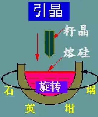
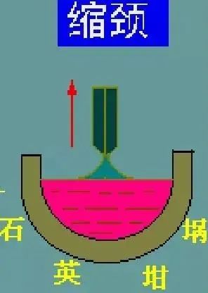
Necking occurs after the nucleation is complete, where the temperature rises, and the seed crystal is rotated and pulled up to obtain a new single crystal with a diameter of 0.5-0.7cm, which is thinner than the seed crystal. The purpose of necking is to eliminate the original defects of the seed crystal or new defects caused by temperature changes during nucleation. The pulling speed during necking is relatively fast, but it should not be too fast. A pulling speed that is too high or a significant change in diameter can easily lead to the formation of polycrystals.
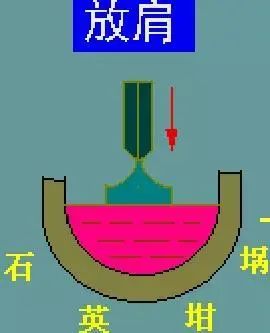
Shoulder release, after necking, the speed is slowed down, and the temperature is lowered to allow the crystal to grow to the required diameter.
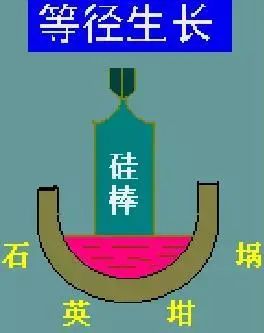
Constant diameter growth, before completing the shoulder release, the temperature is slowly raised, and after shoulder release, the diameter of the single crystal is maintained during growth. During the growth process, both the pulling speed and temperature should be as stable as possible to ensure uniform growth of the single crystal.
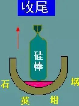
Finishing, as the single crystal growth nears completion, the temperature is appropriately raised, the pulling speed is increased, and the diameter of the crystal rod is slowly reduced to draw out a conical tail. The purpose is to avoid defects extending upward due to rapid cooling when the crystal rod leaves the molten liquid.
Testing the Performance of Single Crystal Silicon
Well-grown single crystal silicon needs to be tested to measure whether various parameters meet the requirements.
Testing Physical Properties
Appearance inspection, crystal orientation inspection,diameter measurement
Defect Inspection
Electrical Parameter Testing
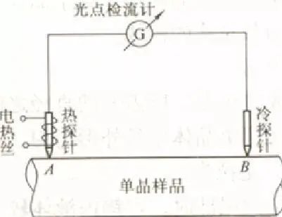
Testing of conductivity types;
Testing of non-equilibrium carriers;
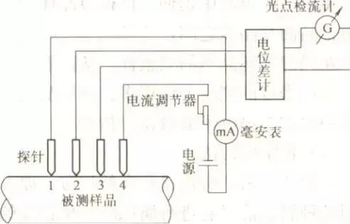
Testing of resistivity.
Source: Semiconductor Materials Circle