Gallium Nitride (GaN), Gallium Oxide (Ga₂O₃), and Diamond are recognized as strategic advanced electronic materials internationally. Among them, GaN, as a representative of wide bandgap semiconductors, possesses excellent material characteristics such as a large bandgap, high breakdown field strength, and high electron saturation drift velocity. It is the core of short-wavelength optoelectronic devices, microwave RF devices, and power devices, and has been widely used in fields such as lighting, displays, 5G mobile communications, consumer electronics, new energy, and national defense equipment, being included in China’s 14th Five-Year Plan.
Technology Activity Week
The history of human lighting has undergone a long and complex evolution, and the development of lighting technology is a microcosm of human civilization. The earliest lighting used natural light sources (sunlight, bonfires, torches), all of which were natural products. In 1879, Thomas Edison invented the incandescent lamp, leading a revolution in human lighting methods. Incandescent lamps are inexpensive, simple, and practical, still in use over a century later, but their main drawback is low luminous efficiency, about 2%. In the early 20th century, Emman invented the energy-saving fluorescent lamp. The mechanism of fluorescent lamps differs from incandescent lamps; it first generates ultraviolet light through mercury vapor discharge, which then excites the fluorescent material on the inner wall of the tube to emit visible light. Fluorescent lamps quickly entered people’s daily lives as a new lighting fixture. However, fluorescent lamps contain harmful elements such as mercury, causing significant environmental pollution. With the development of human economic society, the energy crisis and environmental pollution have intensified, and energy conservation and green development have become a consensus. Countries have accelerated legislation to ban the production and use of incandescent and fluorescent lamps while vigorously promoting energy-efficient lighting to replace traditional lighting. Against this backdrop, efficient, energy-saving, environmentally friendly, and long-lasting semiconductor lighting has emerged. In 1993, based on the invention of the GaN semiconductor blue LED chip, humanity entered a new era of white LED lighting. The inventors of the blue LED, Shuji Nakamura, Isamu Akasaki, and Hiroshi Amano, were awarded the Nobel Prize in Physics in 2014. Incandescent lamps and fluorescent lamps are gradually being replaced by efficient, energy-saving, and environmentally friendly semiconductor LED lamps, and by 2020, China’s semiconductor LED lighting industry scale had reached 1 trillion yuan.

2014 Nobel Prize winners: Isamu Akasaki, Hiroshi Amano, Shuji Nakamura
LED, short for Light Emitting Diode, is a type of solid-state lighting device that uses solid semiconductor chips as the light-emitting material. It emits photons by releasing excess energy through carrier recombination in the semiconductor. By changing the components of the semiconductor material, different colors of light can be emitted, such as red, blue, and green. Therefore, LEDs are widely used not only in lighting but also in displays, illuminating terminal information. Currently, emerging GaN-based Micro-LEDs, high-speed LEDs, and deep ultraviolet LEDs have enormous potential markets in AR and VR micro-displays, visible light communication, and sterilization and disinfection.
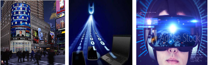
Semiconductor LED large screen display, visible light communication, micro-display
Building on LED lighting and displays, countries are also actively focusing on the research and development of GaN-based semiconductor laser lighting and display technologies. Semiconductor lasers are laser diodes formed on the basis of LED structures through optical resonant cavities. The excitation mechanisms of laser lighting and LED lighting are similar; both use blue light to excite yellow phosphors to achieve white light output. Semiconductor lasers have characteristics such as directional light emission, extremely high brightness, immense energy, and pure colors. Therefore, compared to LED lighting, laser lighting is more efficient, brighter, and has better modulation capabilities. At the same time, using red, green, and blue laser as light sources can be applied to full-color displays. The color gamut of laser full-color displays is wide, covering nearly 90% of the colors recognizable by the human eye, enabling double high-definition (geometric, color) video image display, which is called a “revolution in human visual history,” with vast application prospects and markets in televisions, home theaters, and portable laser projectors.
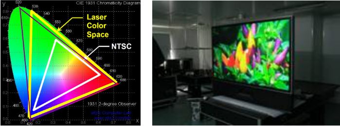
Laser display color gamut range 65-inch large screen semiconductor laser TV
GaN-based semiconductor materials are suitable not only for the preparation of high-performance light-emitting chips but also for the preparation of high-frequency, high-power high electron mobility transistors (HEMTs) due to their wide bandgap, high electron saturation drift velocity, high breakdown field strength, and stable physical and chemical properties. GaN-based HEMTs have output current densities more than ten times higher than GaAs-based electronic chips. High-frequency, high-efficiency, wide bandwidth GaN-based HEMT microwave RF chips have broad application prospects in 5G mobile base stations, phased array radars, satellite communications, and wireless charging. In addition, GaN-based HEMT power electronic chips, which are resistant to high voltage, high current, and low loss, can be applied in smart grids, high-speed rail transportation, and new energy vehicles, with enormous market potential. GaN semiconductors have been classified as “strategic advanced electronic materials” in China and are officially included in the “14th Five-Year Plan.” It is expected that by 2035, China’s GaN-based HEMT chip technology will gradually mature.
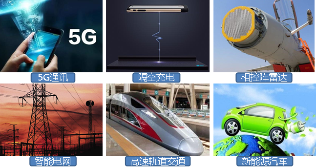
GaN-based HEMT chip application fields
The Wide Bandgap Semiconductor Chip Laboratory belongs to the National Key Laboratory of Integrated Optoelectronics. It is equipped with high-end semiconductor equipment, including a German AIXTRON nitrogen MOCVD system, a self-developed oxide MOCVD system, and a CVD system for diamond growth, providing support for the epitaxial growth and chip development of wide bandgap semiconductor materials such as GaN, Ga₂O₃, and Diamond. Currently, the research team in the laboratory includes 3 professors, 4 associate professors, and 30 graduate students, forming a first-class research team in wide bandgap semiconductors in China. In 2015, the team was approved as the “Jilin Province Third Generation Semiconductor Materials and Devices Innovation Team.” In 2018, the team was approved to establish the “Jilin Province Wide Bandgap Semiconductor Materials and Devices Engineering Laboratory.” In 2020, the team won the first prize of the Jilin Province Science and Technology Award (Professor Zhang Yuantao ranked first). At the same time, the team collaborates with industry leaders such as Huawei to serve the country in achieving key technology autonomy and developing display chips and RF chips for advanced displays and next-generation communication technologies. With the joint support of the Jilin Provincial Development and Reform Commission and Jilin University, the team co-established a wide bandgap semiconductor joint laboratory with Jilin Huamei Electronics Co., Ltd. (the first listed company in the field of semiconductor power devices in China) to jointly focus on the research and industrialization of wide bandgap semiconductor power devices; in collaboration with the listed high-tech enterprise Yuanrong Optoelectronics Technology Co., Ltd., they developed GaN-based Micro LED chips, with Professor Zhang Yuantao as the person in charge. The Micro LED project participated by Yuanrong Optoelectronics received funding from the National Natural Science Foundation’s regional joint fund key project; Professor Zhang Yuantao, as the project leader, collaborates with Suzhou Navi Technology Co., Ltd. on a national key R&D program project, responsible for developing nitrogen-polar GaN-based HEMT devices.
Graduate student destinations include companies such as Huawei, Intel, FAW, SMIC, Hisense, BOE, as well as research institutions such as Peking University, Tsinghua University, Dalian University of Technology, Zhengzhou University, and the Changchun Institute of Optics, Fine Mechanics and Physics, Chinese Academy of Sciences.
Contact information for team leader Professor Zhang Yuantao:
Office: Jilin University Central Campus, Tang Ao Qing Building D261
Email: [email protected]
Contact information for team member Associate Professor Deng Gaoqiang:
Office: Jilin University Central Campus, Tang Ao Qing Building D261
WeChat: 13843122427
Email: [email protected]
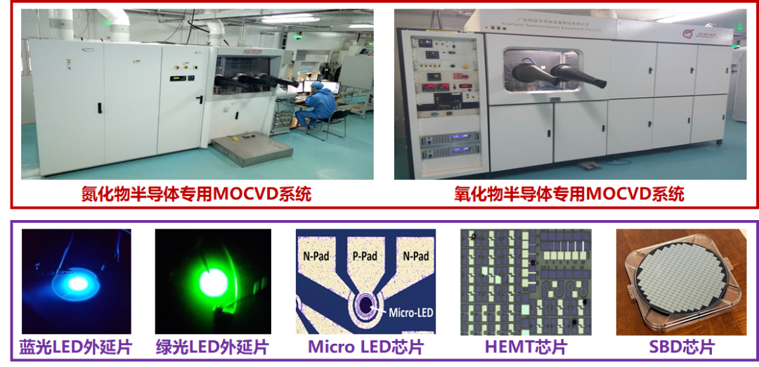
The advanced semiconductor material epitaxy systems and the high-performance Micro LED chips, HEMT chips, and SBD chips developed by the research team of the Wide Bandgap Semiconductor Chip Research Team at the National Key Laboratory of Integrated Optoelectronics, Jilin University.
Text and image editing by | Xu Ziye
Review | Hu Jingyu
Supervisors | Wei Weihua, Lin Bingzi
Editor | Information Technology Center of the School of Electronics
School of Electronics Science and Engineering, Jilin University
Official WeChat Public Platform
WeChat ID: jludzxy
Long press the QR code below to follow us