Table of Contents
✍
Welcome to click here to join the hardware electronics group of San Pao Er.
Hello everyone, I’m San Pao Er; today’s notes are about the RS-232 protocol/interface.
The RS-232 serial data communication interface standard was established by the Electronic Industries Alliance in the United States. This standard defines the electrical characteristics of signals, timing, logic levels, and the physical dimensions and pin definitions of connectors.
1.Interface Types and Signal Definitions
The RS232 standard physical interface has 25 pins, but the commonly used one is the 9-pin connector, which is now basically a DB9 connector.
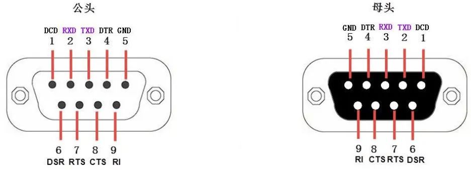
1. DB9 Connector Schematic
2. DB9 Connector Physical Image
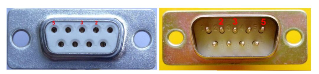
DB9 female and male physical image – with pinouts
3. DB9 Interface Signal Definitions
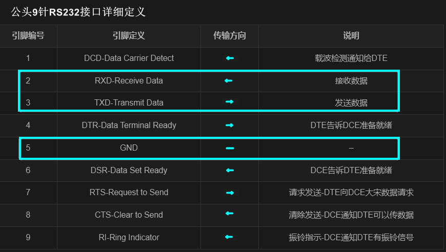
In practical applications, usually only the RXD, TXD, and GND signal pins are used to transmit data directly.
RXD: Used to receive data signals sent by DCE, i.e., input;
TXD: Used to send signals from DTE, i.e., output. The RXD and TXD of the male and female connectors should be cross-connected;
GND: Used to balance the ground potential between both devices, i.e., common ground.
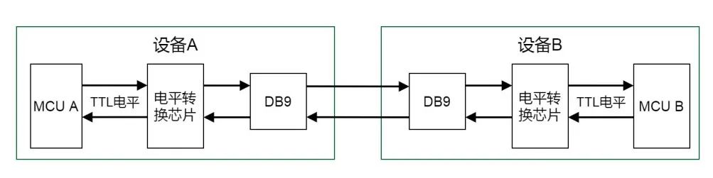
4. DB9 Interface Interconnection
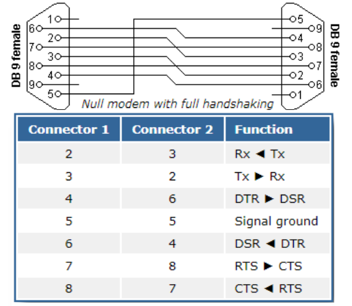
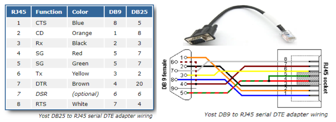
Some designs may also use the RJ45DB9 connection cable shown below, with the physical and signal definitions as illustrated.
2.Logic Levels
RS232 uses negative logic levels.
The logic “1” level is -3V to -15V,
and the logic “0” level is +3V to +15V.
The purpose of choosing this electrical standard is to enhance anti-interference capability and increase communication distance.
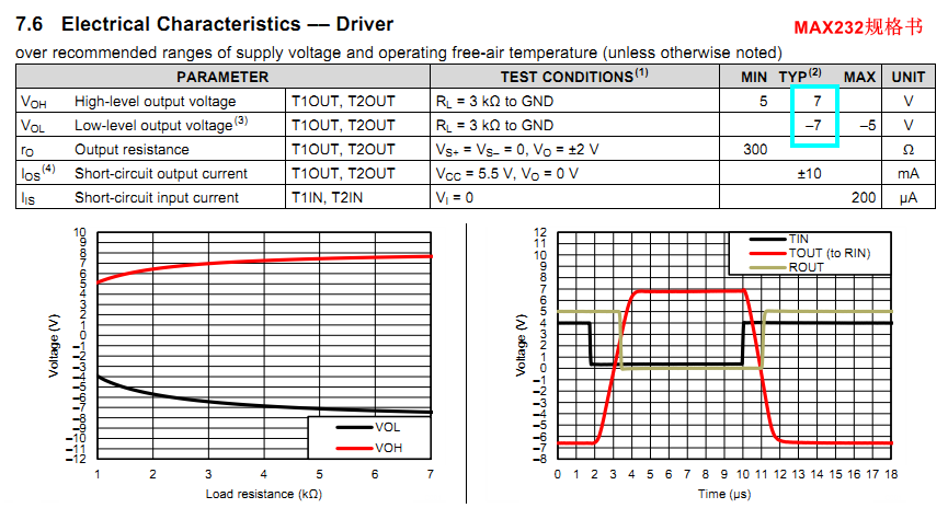
The above levels are just the ranges specified by the RS232 protocol; the actual level ranges of devices fall within this range.
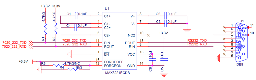
For example, the actual levels of MAX232 are as follows:
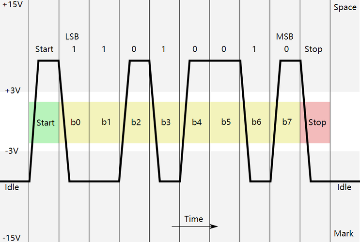
Data is transmitted character by character, with each character transmitted bit by bit, and the transmission of a character always starts with a “start bit” and ends with a “stop bit”; there is no fixed time interval requirement between characters.
Each character has a start bit (transitioning from high to low), and the character itself consists of 7 data bits;
Finally, there is one or one and a half or two stop bits;
During actual transmission, the width of each signal bit is related to the baud rate; the higher the baud rate, the smaller the width. Before transmission, both parties must use the same baud rate settings.
RS232 Level Standards
The logic level for 1 is -3 to -15V, and for 0 is +3 to +15V; the level definitions are inverted once.
The main reasons for converting serial TTL levels to RS232 levels are as follows:
At the moment of device initialization, the IO port is in high-impedance input state, and TX without pull-up may cause dirty data to be sent to the other end.
Our company has specifications requiring that RX and TX be pulled up during circuit design, but only the pull-up resistor for TX is soldered; the pull-up resistor for RX is not soldered.
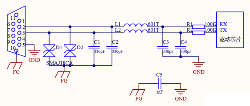
1.D1 and D2 are TVS diodes, which can effectively suppress large energy interference and electrostatic discharge during plugging and unplugging. The parameters used here are SMAJ18CA, and we won’t elaborate on the specific selection methods and precautions;
2.L1 and L2 are ferrite beads that can create high impedance to high-frequency interference. C1 to C4 provide low impedance discharge paths for interference, preventing interference from being transmitted through the RS232 line.
The above points mainly realize the functions of electrostatic protection and suppression of radiation disturbances;
When RS232 is installed outdoors, additional protection against lightning surges and other large energy impacts is required, similar to gas discharge tubes and thermistors in RS485 circuit structures.
2. PCB Layout Recommendations
1.The return path for protective devices is FG (device enclosure), indicating that when the device has a metal enclosure, grounding is managed separately, with FG connected to the board ground through a 1nF capacitor, and FG connected to the chassis nearby; when the device has a non-metal enclosure, FG is directly connected to the board ground, and the device layout is divided into regions;
2.The ferrite beads and TVS components should be close to the board edge or connector end to maximize the filtering of external interference signals at the board interface;
3.No wiring should be done around the interface and its filtering protection circuit.
Signal cables should use shielded cables, and the shielding layer should ensure 360-degree contact with the connector to avoid the “pig tail” effect.

Finally

More Notes
Introduction to Common Level Conversion Circuits
Understanding SPI Interface in One Article
Understanding I2C Bus in One Article
Understanding the Similarities and Differences Between Crystal Oscillators and Crystals, Design Selection
Understanding Xilinx Zynq7000 and 7 Series FPGA Power-on Timing in One Article
Understanding BUCK Circuit Bootstrap Capacitors in One Article
What are the Differences Between LDO and DCDC?
Understanding DCDC Basics in One Article
Understanding LDO Basics in One Article
What Research is There on Pull-up and Pull-down Resistors?
Why is it Common to Place Two Capacitors, 1uF and 0.1uF, in Parallel in Circuits?

This is Soft Grinding HardPao’s WeChat Official Account, where the owner San Pao Er shares hardware development learning notes and experiences.
Learningand sharing to assist in capability growth, exchanging experiences to aspire to be first-class.