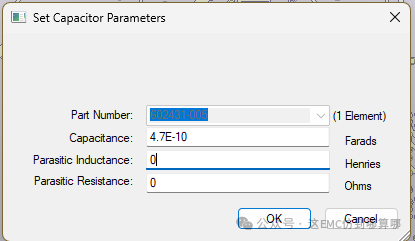
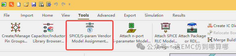
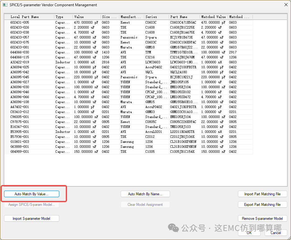
This article introduces resonance simulation and decoupling capacitor placement, applicable during the pre-layout design or rectification phase of power/ground planes in PCB design, to avoid board-wide resonance issues within the concerned frequency range. The software used for this simulation is SIwave from Ansys. The PCB import will not be elaborated here; it is important to ensure that the stacking information and dielectric substrate information are correct, as they significantly impact the simulation results. Additionally, after importing the board, all LC values are ideal; we need to replace them with components from the software library that include parasitic parameters, or if accurate parasitic parameters can be obtained, they can be manually input. The first two images show manual changes to parasitic parameters, while the last two images show the replacement with components from major manufacturers. You can check if the parasitic parameters have been successfully added through the circuit elements properties.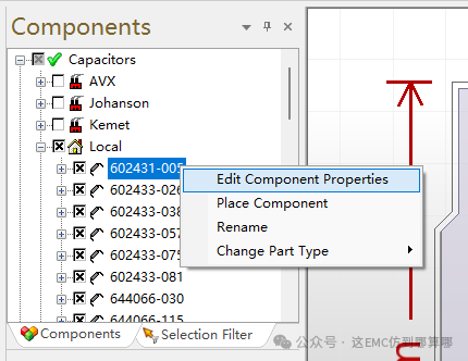

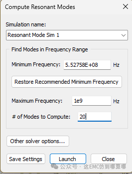
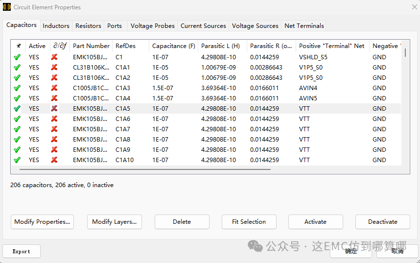 After defining the LC and parasitic parameter values, we perform resonance mode calculations, setting the minimum and maximum frequencies of interest and the number of modes to calculate. The default minimum frequency in the software isthe geometric diagonal length of the board divided by the square root of the dielectric constant, click on other solver options to set simulation accuracy, number of cores to use, etc., and click launch to start the simulation.
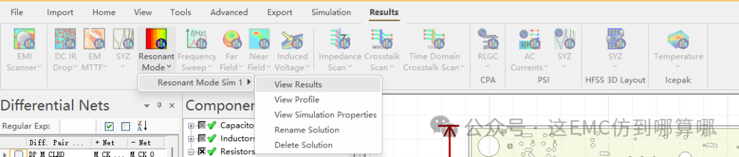
 To view the results: select the main menu Results→Resonant Modes→Resonant Mode Sim 1→View Results.
 Generally, the power plane and ground plane of the PCB are selected to calculate the resonance modes, as a large resonance cavity is formed between these two planes, making it easy for energy to be trapped between the two parallel plates. When the original signal and reflected signal are in phase, a resonance cavity effect is created. If the layers of your power plane or ground plane are dispersed, you need to draw them all out.For each set, SIwave will calculate all resonances between the selected two layers. Then, we must observe each to see which resonance surface belongs to which power plane.
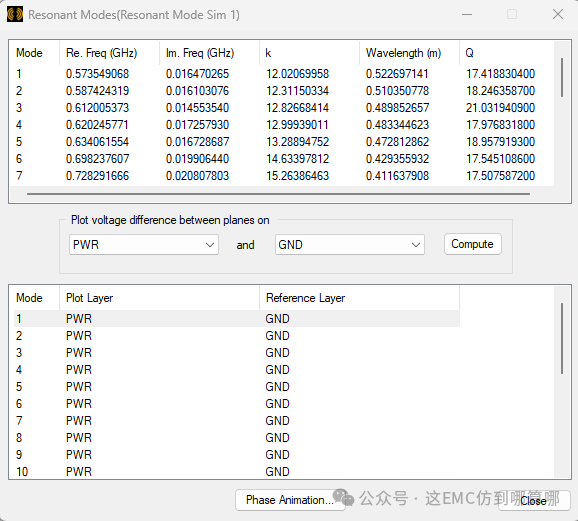 After the calculations, we can check the resonance conditions at various frequency points. The software lists all possible resonance frequencies, and we need to further identify whether rectification is necessary. Some users may not like the grid display and can turn it off through View; for convenience in adding decoupling capacitors later, the voltage cloud display can also be turned off.
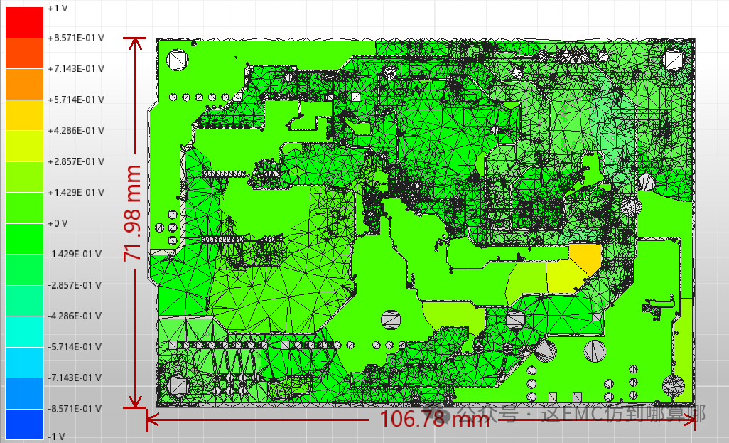 The red and blue colors represent the peaks and troughs of the resonance, respectively, while green indicates areas with minimal oscillation.
 For example, we find a significant resonance around 1006MHz, and we can dynamically display the phase and export animations.
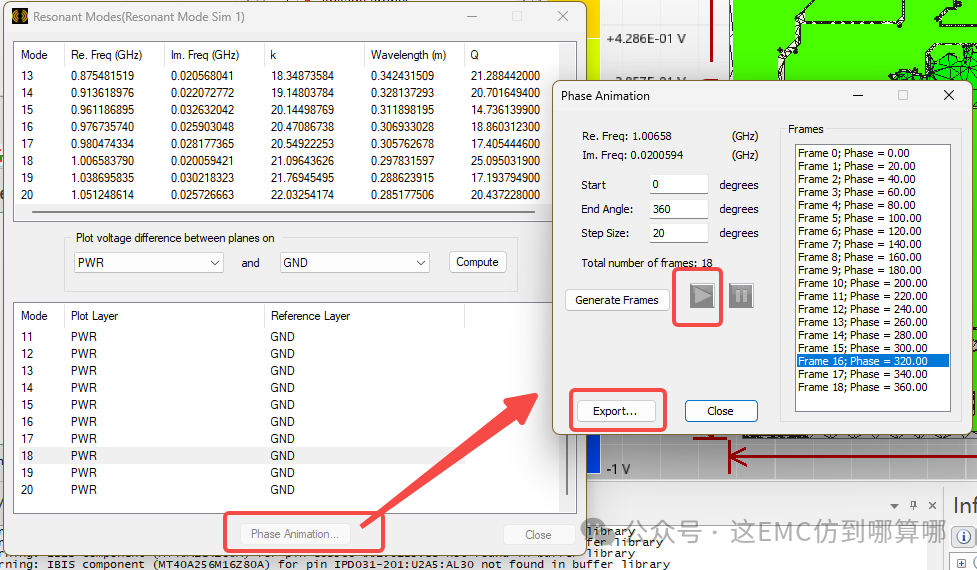 Interpretation: The real part represents the resonance frequency, while the imaginary part represents the loss of the resonance or attenuation factor. k is the characteristic number, equal to the resonance frequency in free space multiplied by 2PI/c (the speed of light), approximately 20.954 times the resonance frequency (in GHz). The wavelength is the wavelength in air, and Q is a measure of the sharpness of the resonance, equal to the resonance frequency divided by twice the imaginary part. (Source: Internet)
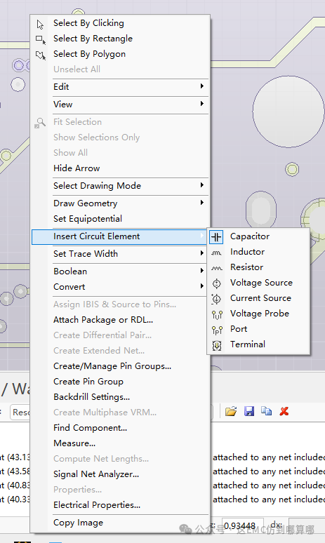
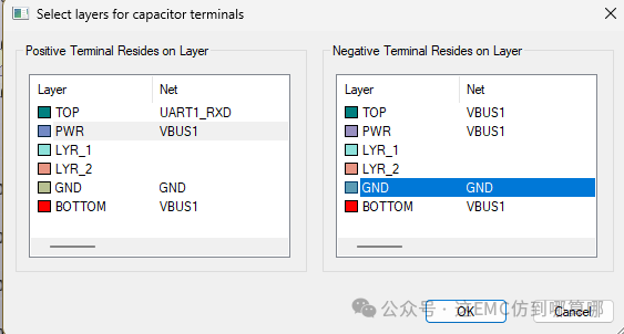
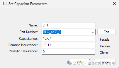
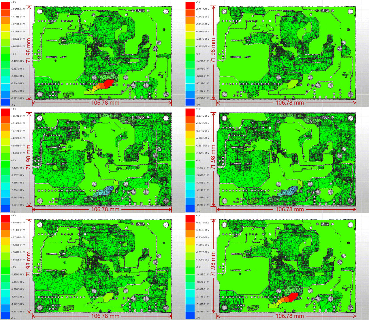 We add decoupling capacitors here to mitigate the impact of resonance. Turn off the voltage display, in the components window, right-click the pre-prepared capacitor and select place component. The capacitor can be placed graphically or precisely by coordinates. After placement, a selection box pops up; select the positive terminal to the power plane and the negative terminal to the ground plane. You can also directly click the icon in circuit elements or right-click to insert the capacitor into the PCB, then assign values to the capacitor.
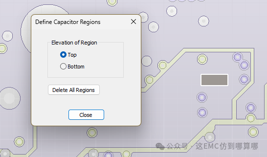
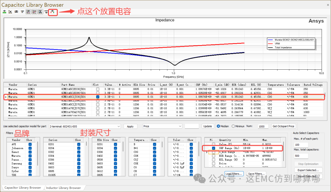
 SIwave also has a function for assisting in LC selection. For example, if the resonance frequency is 1006MHz, we can go to Tools→Capacitor Library Browser to filter for SRF Range around 1GHz, and select the best candidate for the decoupling capacitor based on the filtering results. Here, we introduce the concept of Capacitor Regions; previously, we connected the capacitor directly to the inner circuit board, but this is not feasible in actual circuits (the advantage is that it allows for a quick view of whether the placement of components is effective). Capacitor Regions allow us to draw a rectangular area for the capacitor on the top/bottom, and then we can use the Capacitor Library Browser to filter and place the desired capacitor into the generated area.When filtering decoupling capacitors, pay attention to the capacitor size (to ensure it can fit within the defined capacitor installation area) and the resonance frequency point (to ensure it can effectively decouple).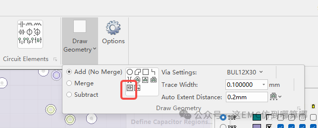
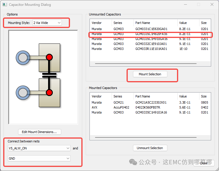 Set the capacitor placement method and pin positions, select the region just set, and click Mount Selection to see the successful placement screen below. If you accidentally place it incorrectly or place too many, you can delete it using Unmount Selection below.
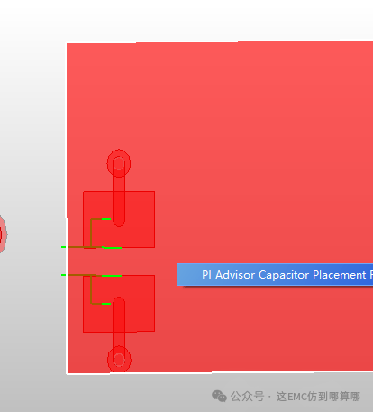 After rerunning the resonance simulation, we find that the resonance frequency point of 1.006GHz is no longer present, and the voltage at nearby frequency points has significantly decreased compared to before, indicating that the decoupling capacitor is effective~ (but we still need to consider whether it affects other frequency points). In addition to adding decoupling capacitors, we can also change the stacking structure and plane segmentation to alter the resonance frequency and distribution, and we should avoid placing critical components and traces on planes with significant resonance at the operating frequency.
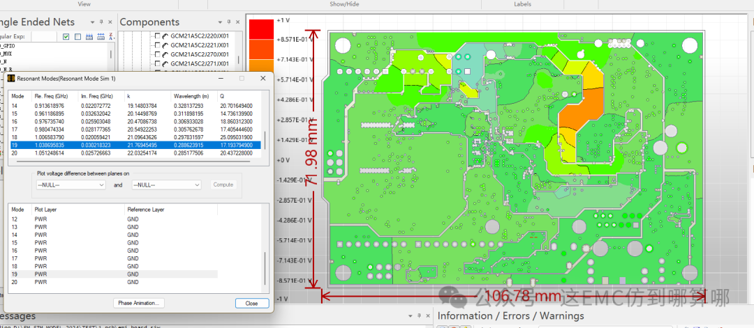 Before adding decoupling capacitors
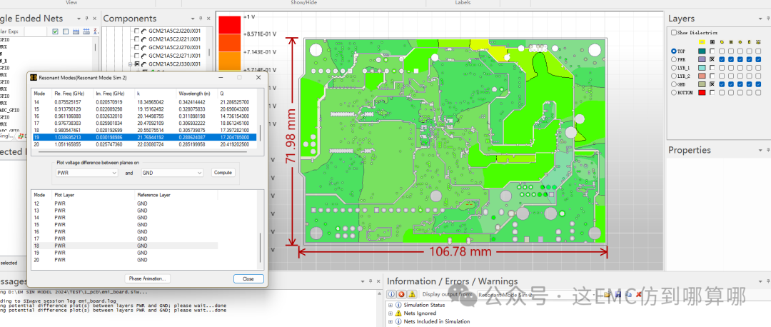 After adding decoupling capacitors Although this simulation is simple and intuitive, we cannot solely rely on the voltage distribution map to determine the severity of resonance. Please note that the red area is always 1V, and all resonances are normalized to 1V. Therefore, using the field map alone to judge the resonance mode is quite radical; we also need to check the impedance curve Z11. Due to the length of this article, we will discuss impedance analysis and the relationship between impedance and resonance in the next article. A small note from the author: if you find this helpful, please consider following, liking, and sharing. I will update the text version of the PI simulation tutorial soon, and if it gets enough views, I will also record an operation video for the public account or the same-name Bilibili account. By the way, is there still interest in SI simulation? Please raise your hand so I can see you!Disclaimer: The PCB model in this example is from an official Ansys case, and some materials are sourced from the internet.