Source: Content from the world of lithographers, thank you!
The history of integrated circuits began with TI’s first Flip-Flop circuit in 1958, which was made up of only two transistors forming an inverter. Today, we have CPUs with billions of transistors, all thanks to the continuous technological advancement in the semiconductor manufacturing industry that allows for scalable production.
The realization of semiconductors mainly relies on their ability to achieve binary conversion of “0” and “1”, starting from the Vacuum Tube hardware. Around the time of World War II, electronic computers began to be utilized mainly for communication and code decryption. However, the performance of these transistors would quickly degrade, increasing troubleshooting time and indirectly hindering the development of the semiconductor industry.
It wasn’t until 1947 that three pioneers at Bell Labs, one of whom was William Shockley, invented the point-contact Ge transistor. Then in 1950, Shockley invented the first BJT. Compared to vacuum tubes, these devices exhibited significantly improved reliability, power consumption, and size. Notably, the BJT is a three-terminal transistor that can act as an electrical switch, with one terminal serving as the control terminal. In 1958, TI’s Jack Kilby created two BJTs on silicon, ushering in the “Silicon Age”. Early circuits were built using BJTs, which operate on the principle that they are current-driven (base current), and since Ice is a bipolar device, it not only drives a large current but also suffers from significant static leakage. Thus, if your circuit is very large, the leakage power loss becomes unacceptable, limiting its applicability.
By 1963, Fairchild Semiconductor invented the CMOS circuit, composed of symmetrical complementary NMOS and PMOS devices, which is the CMOS technology we are familiar with today. Because its control gate is coupled through an electric field across the Gate Dielectric, it does not generate static power consumption from control currents, theoretically allowing for a static power consumption of “0” (though in reality, there is still gate leakage). In fact, early integrated circuits were implemented using only NMOS and BJTs, without PMOS, because Twin Well technology did not exist at that time. By the 1980s, the number of transistors in CPUs had grown to thousands, and power consumption had become untenable, leading to the advent of the CMOS (Twin Well) era.
In the following years, the industry adhered to Moore’s Law, established in 1965, leading to successive improvements in speed, density, and performance. The journey from Bulk-Si to 32nm hit a wall, prompting a transition from planar to 3D FinFET and SOI technologies.
1. MOSFET Devices
MOSFET stands for Metal-Oxide-Semiconductor Field Effect Transistor. The Metal refers to the gate as the control terminal, the Oxide is the gate oxide that senses the electric field to induce the inverted channel, and the Semiconductor is naturally the silicon substrate channel. The Field Effect indicates how it operates; the control terminal generates an electric field through the gate oxide, inducing an inverted channel to allow conduction between the source and drain, thereby achieving the conversion of “0” and “1”.
MOS Structure
MOSFET has a four-terminal structure: gate, source, drain, and body (substrate). The gate is made of low-resistance material, and there is a thin gate oxide layer between it and the substrate channel.Typically, the source and drain are doped with opposite types compared to the substrate and channel (for example, NMOS has N-Type source/drain, while the substrate and channel are P-type), hence the PN junction between the source and drain remains off.However, when a voltage is applied to the gate (NMOS receives positive voltage, PMOS receives negative voltage), an electric field is induced at the surface of the channel through the gate oxide, causing minority carriers from the substrate to accumulate at the channel surface and invert it, thus allowing conduction between the source and drain.The gate’s threshold voltage (Vt) is determined by the work function of the gate and substrate, as well as the thickness/quality of the gate oxide and the doping concentration of the substrate.
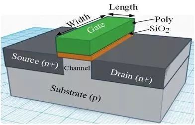
Why Use Poly as Gate Material
Originally, the gate material for MOSFETs was aluminum, which is why it was called MOS rather than POS. Later, it evolved to poly. This was mainly due to the fact that Metal Gate processes are “Gate Last”, where the source/drain are made first and then the aluminum gate is added. However, this poses a problem as the gate and source/drain must have a certain overlap to ensure a connection (typically a 0.5um overlap for 2.5um aluminum gate MOSFETs). This overlay capacitance (Cgs/Cgd) increases the total Miller capacitance, slowing down circuit speed.
To resolve the gate and source/drain overlay capacitance issue, self-aligned sources and drains must be used, where the gate is made first and then serves as a mask for the source/drain implant, achieving self-alignment; this is known as the “Gate-First” process.
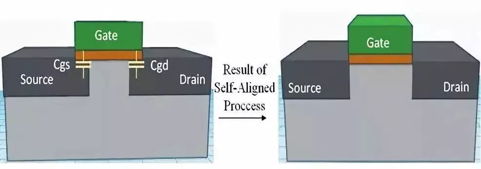
However, the “Gate-First” process also has its own issues, as the doping of the source and drain must be activated at temperatures above 800C. If the original aluminum gate is used, it cannot withstand the high temperature (pure aluminum melts at 660C, and AlSiCu alloys have melting points < 500C). Therefore, poly was adopted as the gate material for the “Gate-First” process, but poly has high resistance, leading to the development of doped poly.
Additionally, another reason for switching to poly as the gate material is the work function; the work function of metals is too high, causing Vt to reach 3~5V, which was acceptable in earlier MOSFETs but certainly not in the submicron era. Thus, poly can be doped to adjust the work function and consequently Vt.
Working Principle of MOSFET
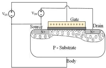
The key to MOSFET operation lies in the gate, which controls the opening and closing of the source and drain. It functions like a faucet switch. Taking NMOS as an example (source/drain are N-type, channel and substrate are P-type), when a positive voltage is applied to the gate, the substrate couples to induce minority carriers at the channel surface until it becomes inverted, allowing the source and drain to connect. Throughout this process, the N-type of the source/drain and the P-type of the substrate must be zero or reverse-biased (source and body grounded, drain receiving positive voltage), making it a PN-junction isolated device.
Small Dimension Effect
Quoting a passage from “Fundamentals of Microelectromechanical Systems” (Page-9), “Not everything performs better when miniaturized; some physical effects that can be neglected in macroscopic devices become prominent at microscopic sizes, which is the law of scaling. For example, a flea can jump many times its height, while an elephant cannot.”
For MOSFETs, when the drain is reverse-biased, the depletion region of the PN junction widens and extends into the channel region, thus the effective channel length Leff = Lpoly – 2 * Depletion. If the channel length is sufficiently long, then Leff is approximately equal to Lpoly; however, when Lpoly is very short, the proportion of the depletion region becomes significant and cannot be ignored, leading to short-channel effects.
Next, we will discuss a series of issues arising from proportional scaling:
Carrier Velocity Saturation and Mobility Decrease
The velocity of carriers in the channel is related to the electric field in the channel. When the electric field increases, the velocity will eventually saturate, which is known as the velocity saturation effect. This is why the saturation current does not increase with rising drain voltage.Additionally, at high electric fields, carrier scattering becomes severe, leading to a decrease in mobility, and interface scattering at the oxide layer can also be significant, further reducing carrier mobility.
Leakage Voltage Reducing Barrier
Another problem brought by short channels is that the drain voltage alters the surface barrier of the channel, reducing Vt. For long-channel devices, the channel barrier is determined by the gate voltage Vg, while for short-channel devices, the channel barrier is determined by the gate-source voltage (Vgs) and gate-drain voltage (Vgd). If the drain voltage increases, the depletion region of the drain PN junction extends laterally into the gate area, so under low Vg conditions, the surface barrier of the channel decreases due to the increased electric field, allowing carriers to bypass it, which is also known as subthreshold leakage. For more details, see “Theory of MOS Devices – DIBL, GIDL”.
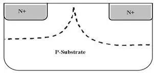
Source-Drain Punch-through
This seems similar to DIBL, as it is also a problem caused by the drain voltage, where the width of the depletion region extends into the channel and inadvertently meets the depletion region of the source. Unlike DIBL, which alters Vt based on the channel barrier, this one pertains to the source leading to leakage.
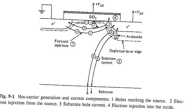
Hot Carrier Effect
This follows a similar logic; as the channel length decreases and the electric field increases, if the drain voltage rises, it leads to an extension of the depletion region closer to the source, further enhancing the lateral electric field at the source-drain junction. This causes vigorous collisions among channel carriers, generating many electron-hole pairs. Under the influence of the gate voltage, these pairs enter the substrate, forming Isub. Why is it called the hot carrier effect? Because the increased electric field accelerates carriers, increasing their kinetic energy and thus their temperature, though you may not feel it. Typically, NMOS is more powerful than PMOS because electrons have a smaller mass and higher speed compared to holes, which have a larger mass and lower speed; thus, kinetic energy E = 1/2 * m * v^2 dominates.
Innovations in the Scaling Era
Mobility Accelerator: Strain Silicon
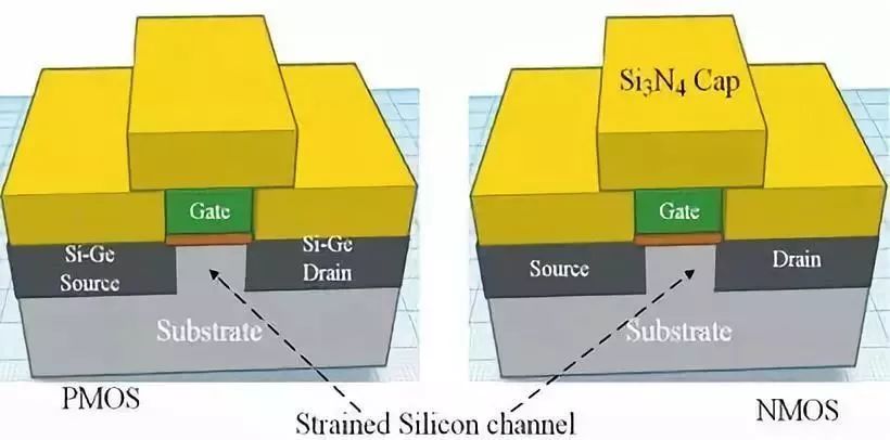
As mentioned earlier, the decrease in carrier mobility due to device miniaturization is not without solutions. We can use a thin layer of germanium (Ge) in the channel to enhance carrier mobility or experiment with strain silicon to introduce channel stress that enhances carrier mobility. Strain silicon technology includes using tensile and compressive stress to improve carrier mobility, thus enhancing transistor performance. For example, PMOS hole mobility can be enhanced through compressive stress in the channel, a method adopted below 45nm as seen in “Strained silicon — the key to sub-45 nm CMOS”.
To manufacture strain silicon in the channel, a Si-Ge layer (20% Ge + 80% Si mixture) is epitaxially filled outside the source/drain region. Since Ge atoms are larger than silicon atoms, this creates compressive stress directed towards the channel, enhancing hole mobility, consequently improving current driving capability and circuit speed. This technology was first employed by Intel in 2003 for 90nm CMOS, enhancing PMOS current driving capability by 25%. This source/drain embedded Si-Ge technology is referred to as e-SiGe (Embedded-SiGe) technology. However, strain silicon technology can only enhance PMOS; what about NMOS? For electrons, tensile stress is required to enhance their mobility, and embedding SiGe in the source/drain is not feasible. Instead, embedding it beneath the channel can also create tensile stress, but the implementation of this process is nearly impossible. Therefore, another method was developed to increase tensile stress around NMOS by adding Si3N4, allowing devices to generate either compressive or tensile stress entirely, or different types of stress for PMOS and NMOS respectively. However, using SiN-induced stress can significantly affect the mismatch of the poly space (the reason for which I still do not know).
Speaking of strain silicon, this seems to be a 12-inch theoretical concept, far removed from us, right? In fact, 8-inch technology also faces this issue. In our 0.18um and below technologies, there is an effect called LOD (Length of Drain/Diffusion), which refers to the distance from the edge of the source region to the edge of the channel along the channel length “L” affecting device current, as illustrated by the distances SA and SB below. This effect is included in SPICE simulations in BSIM 4.0 and above, so when simulating analog circuits that are sensitive to mismatch (such as current mirrors, differential pairs, ADC/DAC circuits), parameters SA and SB must be included, or else one might complain about poor mismatch from the fab later.
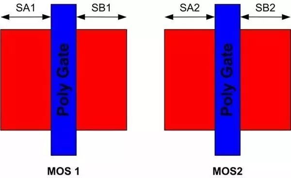
What is the reason for this? Mainly because the surrounding STI and the HDP Oxide generate compressive stress, which, according to e-SiGe theory, will increase PMOS carrier mobility while decreasing NMOS carrier mobility. Consequently, PMOS saturation current increases while NMOS saturation current decreases, as seen in the I-V curve below.
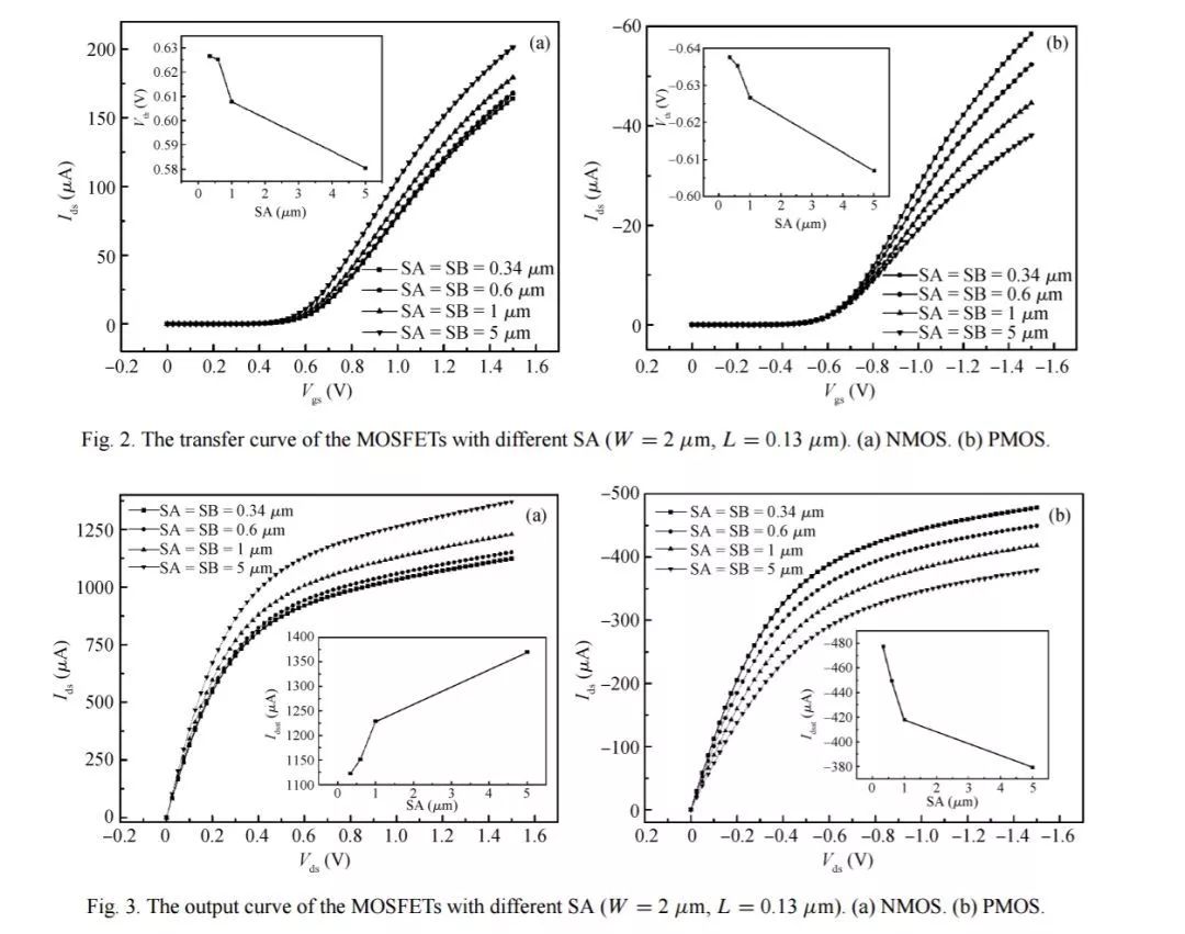
Then the question arises: if we make SA and SB identical, wouldn’t that solve the problem? In the realm of simulation, you will never understand!
Assuming a MOS has two gates forming a multi-finger structure, it becomes even more complex. Here we need SA11=SA21, SB11=SB21, SA12=SA22, and SB12=SB22 for MOS1 to equal MOS2.
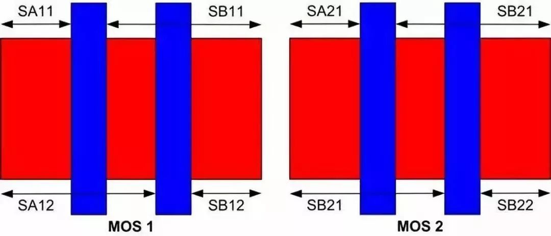
If we further place MOS1 and MOS on a large OD, there would be no issue. But what about the outermost SA and SB? How can we eliminate the impact of LOD? We can only enlarge the OD, typically requiring SA or SB >= 5um, or simply not using the outer MOS, which is the dummy gate.
<pthus, causes="" devices="" in="" introduction="" mismatch.
Gate Leakage: High-K
The thickness of the gate oxide layer has been continuously reduced with proportional scaling, and by 65nm, an effective oxide thickness (EOT) of about 23A (physical 16A) is required. Going further down, it becomes thinner than the natural oxide layer, making direct tunneling (Quantum Mechanical Tunneling) leakage unbearable. Looking back, why do we need to thin it? Because we want to achieve higher transconductance to induce channel inversion, which comes from capacitance. To increase capacitance, we either reduce thickness or increase dielectric constant. Since reducing thickness is no longer feasible, we switched to a higher dielectric constant material. Thus, High-K gate dielectric materials were developed.
The breakthrough of High-K gate materials came in 2007, first introduced by Intel at 45nm using HfO2 (Hafnium), which has a dielectric constant of 25, compared to 3.9 for SiO2. Compare for yourself!
Poly Depletion Effect: Metal Gate
I recall mentioning HKMG in a previous article. If the gate material is polycrystalline, its doping changes with the gate voltage, where the doping near the gate oxide is pulled up by the electric field, while the bottom, which is nearly undoped poly, turns into an insulator, effectively increasing the oxide thickness and lowering transconductance. Of course, aside from switching to High-K materials, using a metal gate is also an option, but it cannot be aluminum, as it cannot withstand the high temperatures required for source/drain activation. Thus, it must be a refractory metal with an appropriate work function; otherwise, Vt will not be maintained.
Like High-K materials, Metal Gate was also first introduced in mass production by Intel at 45nm, proving Intel’s prowess.
Device Structure Innovations
The previous discussions have focused on traditional MOS structures and the various problems and solutions encountered during scaling. However, there comes a point where traditional methods are insufficient, leading to the necessity for new structures! This includes the currently popular SOI and FinFET technologies, aimed at maximizing Gate-to-Channel capacitance while minimizing Drain-to-Channel capacitance.
SOI Technology
The primary difference from traditional MOS is that there is an oxide isolation at the bottom of the well, hence it is called Silicon-on-Insulator (SOI), while still being a traditional planar structure. Its structure consists of three parts: the top silicon is the device portion, the middle oxide serves as insulation, and the bottom silicon is for support, also known as “Handle Silicon”.
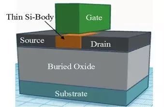
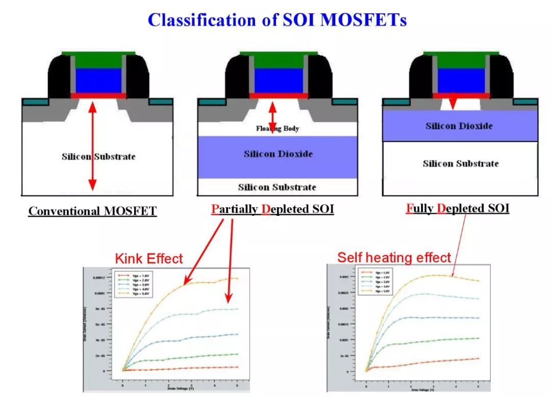
From a structural perspective, there are two types: one is called PDSOI, and the other is FDSOI. The former has a surface silicon thickness almost equal to the depth of the PN junction, so the source/drain PN junction’s depletion region is isolated by the Buried Oxide, effectively reducing leakage and parasitic capacitance, resulting in faster circuits. However, when the gate depletes and inverts, the surface channel is only a few hundred angstroms thick, meaning that some of the silicon beneath the channel still belongs to the well/bulk, so this SOI technology is referred to as partially depleted SOI (PDSOI: Partial Depleted).
This raises a question: if the bulk surrounding the PDSOI is isolated, what happens if the bulk electrode is not connected? Yes, the floating body effect occurs, leading to a drop in Vt and an increase in current, which results in a curve where the current rises sharply; this is known as the kink effect. To resolve this issue, the substrate can be connected, sacrificing a bit of area. To solve the floating body problem without extending the bulk connection, one can ensure that the entire inversion region is fully depleted, which leads to FDSOI (Fully Depleted), resulting in even smaller junction capacitance and faster operation, also referred to as RFSOI. However, this is not without its challenges; creating such thin SOI (~200A) silicon is very difficult, and leakage at the silicon/BOX interface can lead to channel leakage, along with significant self-heating in the channel.
FinFET
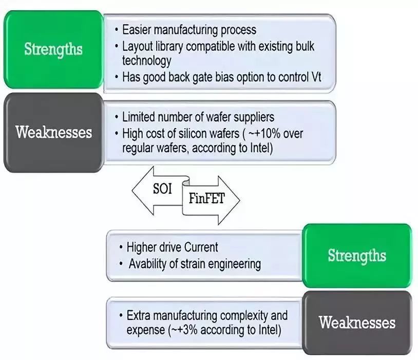
Lastly, let’s discuss FinFET in relation to SOI. If SOI could replace FinFET, that would be ideal, as it remains a planar technology and is more mature. Additionally, it can control Vt through back-gate connections to the BOX, which is advantageous in multi-Vt and low power applications.
In the future, I look forward to even more advanced device structures and manufacturing technologies, as the technology is far from over! For instance, carbon nanotubes, nano-wire FETs, FinFET combined with compound semiconductors, etc.
Recommended Reading:
Issue 98 of International Masters Lecture
Modern and Future Integrated Circuit Electrostatic Protection: Challenges and Solutions
(September 26-27, Shenzhen)
Issue 99 of Masters Lecture
Silicon-based High-Performance Transceiver Clock and Local Oscillator Generation Technology
(October 22-23, Shenzhen)