The role of the capacitor in the 3.3V voltage regulator circuit
Generally speaking, the input capacitor of a 3.3V voltage regulator chip is for filtering, while the output capacitor is to prevent oscillation and maintain voltage regulation performance. However, this is not an absolute rule; as chip designs improve and processes become more sophisticated, some chips can operate without capacitors, and you may not immediately notice any issues. I have conducted experiments to confirm this. Nevertheless, from a practical application perspective, it is still better to include capacitors for safety! There are already chips that can work stably with a 1uF capacitor, which does not take up much space on the circuit board.
Typical circuit diagram and analysis of the 3.3V voltage regulator
The diagram below is the typical schematic of the ASM1117-3.3V. Since I chose the four-pin schematic, I will present the typical circuit for the four-pin version:
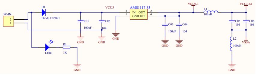
Today, while drawing the circuit diagram for the SD card module, I discovered that the operating voltage of the SD card is 3.3V. Therefore, it is necessary to use a voltage regulator chip to convert the 5V power supply to 3.3V. I looked up some information about voltage regulator chips.
The voltage regulator chip we selected is the ASM1117-3.3, with a SOT-223 package.
However, while drawing the schematic, I encountered a problem. We found two types of ASM1117-3.3V chip schematics in the library, namely:
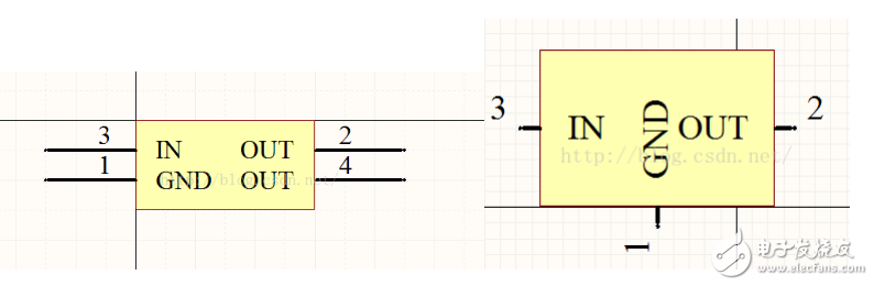
The first type is the four-pin version, while the second is the three-pin version. However, upon checking the packages, both schematics are SOT-223, which is a four-pin package. The issue that puzzled me was why the three-pin schematic could correspond to a four-pin package. I later resolved this confusion by looking at the chip manual. It turns out that pins 2 and 4 of the chip are connected, so it does not matter if the three-pin schematic corresponds to a four-pin package.
While drawing this circuit, we also encountered a problem regarding the component position of the inductor between the network labels VDD3.3 and VCC3.3. Initially, we could not determine this component’s specification, as we found many ASM1117-3.3 circuits, some using inductors and others using resistors. After carefully reading the chip manual and consulting knowledgeable teachers, we learned that this component can be included or omitted without significantly affecting the circuit.
Below is an analysis of the circuit:
1. The role of D1 is to prevent reverse polarity of the power supply.
2. C01 and C02 are for power input filtering.
3. VDD3.3 is the 3.3V power supply used for digital circuits.
4. L1 and L2 are isolation filtering inductors.
5. VCC3.3 is the 3.3V power supply used for analog circuits.
The advantage of isolating the voltage regulator chip into a module is that all peripherals can be directly connected through network labels when level conversion is needed, without needing to redraw the circuit. This saves both drawing time and component costs.
In addition to the 3.3V voltage regulator chip, a 2.5V voltage regulator chip was also used in this project. The circuit connections are very similar, so I will not elaborate further.


To help everyone learn better, ChangXue Electronics Network has specially added a public account for microcontrollers and EDA, pushing relevant knowledge daily, hoping to assist your learning!