
1. Is the on-chip RAM exhausted?
Two different STM32 users reported similar issues. While compiling example projects from the STM32F7Cube library, they encountered a puzzling message indicating that the on-chip RAM was nearly depleted. Given their understanding of the basic functionalities of the project, this shouldn’t have been the case, and they wanted to know what was happening.
The specific situation is as follows: they first opened an example project related to lwip application in the STM32CubeF7 firmware library. For example, a project located in the following directory, which was compiled using ARM MDK.
\STM32Cube_FW_F7_V1.15.0\Projects\STM32746G-Discovery\Applications\LwIP\LwIP_HTTP_Server_Netconn_RTOS\MDK-ARM.
As a result, the compilation indicated that the on-chip RAM space was almost exhausted. However, they felt that such a large amount of RAM memory should not be needed. The client also wanted to add other user programs, which would require using RAM.
After opening the corresponding software project and compiling it using ARM MDK, the compilation results were consistent with the feedback from the client.
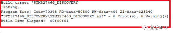
From the compilation results, it seems that RAM was indeed used up by more than 320 KB. So where did that RAM go? By opening the corresponding MAP file for further inspection, we obtained the following data.
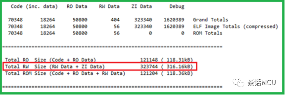
First, let’s take a look at the internal RAM situation. The chip currently in use is the STM32F746NG, and by checking its datasheet, we can see that its internal system RAM capacity is 320KB【1KB=1024B】, consisting of the following three RAM areas, with their capacities and address ranges as follows:
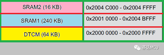
Combining the compilation results and the above data, it appears that RAM is indeed exhausted. Since this is the case, we have no choice but to continue looking at other details in the MAP file, to see where the RAM is being consumed. Later, it was discovered that there was a large PAD patch fill area in a certain address range.
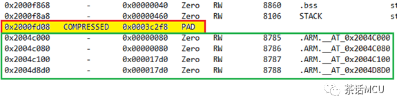
From 0x2000fd08 to 0x2004bfff in this area, a total of 246,520Bytes【which is indicated by the yellow area in the above image】.
Generally speaking, the PAD patch blocks generated after code compilation are often due to address alignment issues, leading to some unusable scattered memory fragments. Normally, these patch blocks should not be concentrated in large areas.
For instance, using the structure variable below will insert padding.
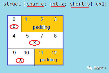
However, the patch block indicated here is excessively large, exceeding 200 KB and is also continuous space! It feels like there is some misunderstanding. From the analysis, it is initially judged that this PAD area should still be usable by the user. Thus, an attempt was made to randomly increase an effective usage of 16KB of RAM in the existing code, and everything compiled normally, with the memory usage results displayed after compilation being almost identical to before, still indicating that RAM was exhausted.
However, by checking the MAP file, it can be found that the aforementioned large patch block space also reduced by 16KB. Clearly, the RAM was not truly exhausted, but the compiler regarded it as a patch block due to alignment reasons. Now the question is, how could the compiler misjudge it as such a large patch block?
By further checking the MAP and some source code files, we can find that a block of RAM area, specifically the SRAM2 area in the chip, has been allocated for memory usage by the user using the attribute keyword, meaning this memory space is not assigned by the compiler. 【In the green box in the figure below, the memory allocation is shown.】
Based on the above analysis, that enormous pad area is actually the end address of the RAM space allocated for use by the compiler up to the start address of SRAM2【0X2004C000】.
This brings to mind a place, which is in the MDK IDE options configuration under the Target configuration:
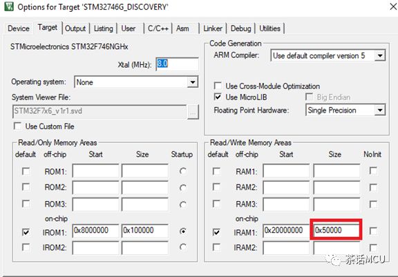
The configuration for on-chip RAM is as follows, which means that all RAM space from 0x20000000 to 0x2004ffff is managed by the compiler.
In actual application code, the compiler starts allocating memory from 0x20000000, while the SRAM2 area is arranged for user use. In this way, the unallocated area from the end of the RAM allocated by the compiler to 0x2004BFFF is regarded as the pad area. It seems to be just a misunderstanding.
So how can we eliminate this misunderstanding? We can slightly modify the above memory configuration item to prevent the SRAM2 area from being managed by the compiler, thus avoiding the space from the end of the memory allocated by the compiler to the start address of the SRAM2 area being regarded as the patch area. Modify it as follows:
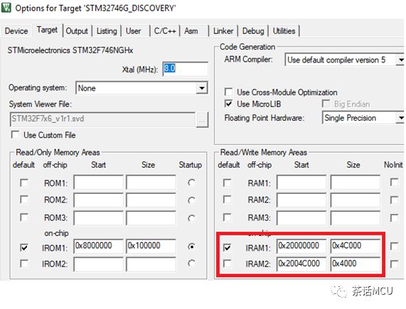
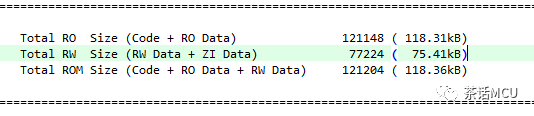
After making this modification and recompiling, the results are as follows, no longer giving the impression that the RAM is fully used, only using over 70 KB of on-chip RAM.
2. Unable to use Flash programming algorithm?
When someone is developing products using STM32F7, they find that they cannot find the appropriate Flash algorithm file during compilation, or the existing FLM files provided by MDK are unusable. The specific situation is as follows:
Someone using STM32F750V8 for product development, after compilation, attempted to download for debugging, but the program could not be downloaded, indicating a FLASH download error.
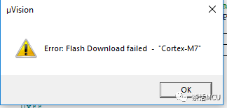
After checking various configurations, it was suspected that there was an issue with the FLASH algorithm file.
Opening the MDK options configuration for the flash_download programming configuration page, it was found that the relevant FLASH programming algorithm files had already been added.
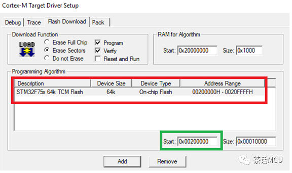
However, for those who have developed with STM32 chips, they may notice something rather glaring: the starting address. For those who have used STM32F0/F1/F4 series, it is easy to notice that the FLASH starting address is generally at 0x8000000, but here it is 0x00200000. Let’s take another look at the MDK options configuration regarding memory allocation:
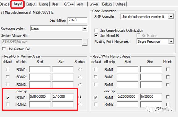
The default starting address for on-chip FLASH is set to 0x8000000. Clearly, this is inconsistent with the starting address definition of the FLASH programming algorithm file, and it is initially judged that this is the cause of the problem.
At this point, it is necessary to check the relevant technical documentation for STM32F7 regarding internal FLASH address allocation. The following diagram shows the framework of the STM32F750 internal master-slave peripherals and buses. For the internal FLASH, the CPU can access it through two bus paths: one is via the AXIM interface, accessing through the AXI-AHB bridge with a 64-bit bus, and the other is through the ITCM interface, accessing it after the internal ART accelerator. 【As shown in the diagram below】
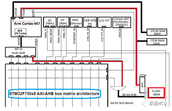
By further reviewing the documentation, it can be seen that when the CPU accesses this FLASH area, different address access areas are arranged depending on the bus interface used.
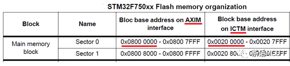
From the table above, it is clear that the address accessed by the CPU when accessing the internal flash via different interfaces is different. The starting address for accessing internal flash through the AXIM interface is 0x0800000, while the starting address for accessing internal flash via the ITCM interface is 0x00200000.
Combining this with the previous case, the inconsistency between the on-chip FLASH address arrangement in the MDK options configuration and the address defined in the Flash algorithm resulted in a program download failure. Therefore, we can adjust the addresses and sizes of both to be consistent, specifically according to actual development needs, based on which interface you want the CPU to use to access the FLASH.
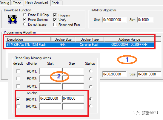
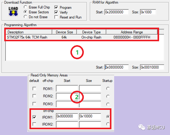
1. If you wish to access through the ITCM interface, we will set both the starting address of the FLASH storage in the Target page and the starting address defined in the FLASH algorithm file to 0x00200000, as shown in the diagram below:
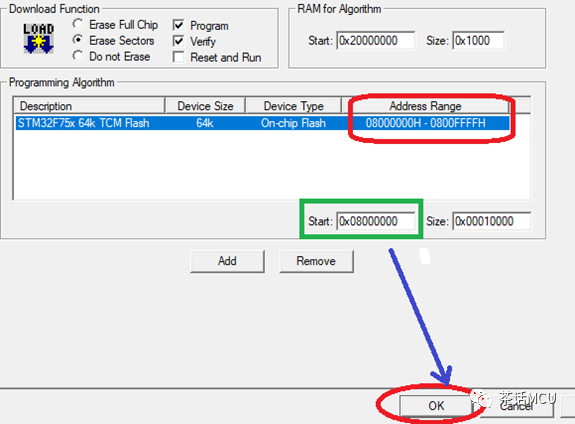
2. If you want to access through the AXIM interface, we will ensure that the starting address defined in the FLASH algorithm file is consistent with the one defined in the Target page, which is 0x08000000.
Based on the FLASH algorithm files provided by MDK, we can directly modify their starting addresses and sizes.
For example, if the algorithm file just loaded is based on the ITCM interface address definition, as shown in the diagram below.
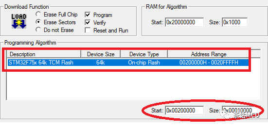
We can directly modify the starting address based on the parameters of the above algorithm file, that is, modify the starting address data in the ellipse, and after completing the modification, click the OK button below to confirm. The operation is shown in the diagram below:
[Note: The version of the ARM MDK I used is 5.28.]
After the modified configuration, recompiling will allow for download and debugging.
Well, the above shared two small reminders during the development process of STM32 in the ARM MDK integrated development environment. I hope you find it helpful.
*********************************************
*********************************************
Previous topic links 【Click to view】:
1. A case of abnormal SPI communication function
2. Timer comparison output switch to achieve custom waveform example
3. Example of master-slave configuration for multiple timers synchronized output
4. A case of application exception related to address alignment
5. Sharing two or three cases of obstacles in STM32 development and debugging