Recently, the presence of the PCB industry has become increasingly prominent. The rumors of Tesla’s Robotaxi, the explosive sales of Xiaomi’s YU7, the Huawei Mate X7 foldable screen, and the spectacular moments of robots playing football all tell us one thing: The more advanced electronic devices become, the greater the demand for PCBs.
Domestic manufacturers are also not idle, rapidly expanding high-end production capacity, which can be described as a “great revolution” in circuit boards.
Meanwhile, NVIDIA’s performance is simply “top-tier”. Its stock price continues to hit new highs, with a market value soaring to $3.8 trillion, reclaiming the title of the world’s largest company. Its AI server orders are booked until 2026, driving numerous PCB manufacturers to operate at full capacity, almost around the clock.
In summary: AI is fluid, but PCBs are solid.
Today, we will discuss PCBs, known as the “mother of electronic products”, from six aspects: ① Basic knowledge; ② HDI and IC substrates; ③ Market and competitive landscape; ④ Development history; ⑤ Industry chain analysis; ⑥ Key segments.
1. What exactly is a PCB?
Don’t be put off by the complexity; PCB stands for Printed Circuit Board. Its role is particularly critical:
-
It provides support for electronic components;
-
It connects various small parts to form a complete circuit;
-
It marks symbols for easy installation and debugging.
Almost all electronic products you can think of, such as mobile phones, computers, automotive devices, and military aerospace, have PCBs in them, which is why it is called the “mother of electronic products”.
Why are most PCBs green?
There are three reasons:
-
Low cost; green ink is the most commonly used;
-
Eye-friendly, making it easier to inspect;
-
Safe and environmentally friendly, reducing the risk of short circuits.
There are many classification methods
-
By material: organic boards, inorganic boards;
-
By flexibility: rigid boards, flexible boards, rigid-flex boards;
-
By layer count: single-layer, multi-layer.
For example, flexible boards (FPC) can bend and fold, commonly found in foldable phones and cameras. Rigid boards are more common, such as the familiar glass epoxy board FR-4, which is cheap and durable.
What does a PCB look like?
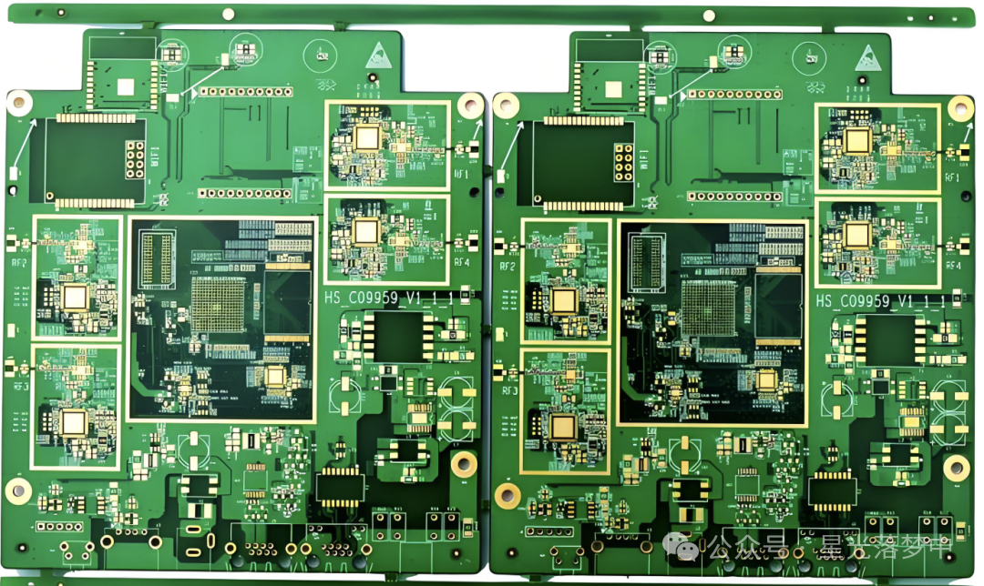
Simply put: copper foil (conductive layer) + core material (insulating layer) + prepreg (bonding layer) + solder mask (protective film), layered like a sandwich.
2. HDI and IC substrates: Key roles in the AI era
1. HDI: High-Density Interconnect Board
Now, smartphones, tablets, and AI devices cannot do without HDI. Its characteristics are light, thin, and small, relying on blind/buried hole technology to achieve higher circuit board density.
In AI computing power, the role of HDI is particularly significant.
-
It can shorten the interconnection bandwidth between chips, improving operational efficiency. For example, NVIDIA’s GB200 uses this technology, achieving an interconnection bandwidth of 1800 Gb/s between GPUs.
-
It can also enhance chip performance by reducing line width and hole diameter.
Therefore, as computing power becomes stronger, HDI is essential.
2. IC substrates: The “base” for chips
IC substrates, also known as packaging substrates, serve to connect chips to the PCB motherboard, acting as a bridge. They not only connect but also support, dissipate heat, and protect.
Compared to ordinary PCBs, IC substrates have higher requirements, achieving thinner and more precise designs. Especially in the high-end packaging field, the cost share of IC substrates can reach 70-80%.
Currently, the high-end market is mainly dominated by manufacturers from Taiwan, South Korea, and Japan, while domestic companies primarily produce mid-to-low-end products. However, with the explosive demand for AI and smart driving, opportunities for domestic alternatives will continue to grow.
3. Market and competitive landscape
1. Global market
According to Prismark’s forecast, by 2027, the global PCB market size will reach $98.4 billion, with an average annual growth rate of about 6%.
The Chinese market is performing even more robustly, with the scale expected to grow from 226.7 billion yuan in 2019 to 346.9 billion yuan by 2024, with a CAGR of 9%.
However, the industry concentration is not high, with the top ten global companies holding only 36% of the market share, and the leading company, Unimicron, only accounting for 7%.
2. Production capacity focus in Asia, with China leading
Although Europe and the United States started early, production capacity has now shifted to Asia, with China being the world’s largest producer. It surpassed Japan as early as 2006, and its position is becoming increasingly stable.
It is expected that by 2026, the PCB output value in mainland China will reach $54.6 billion.
3. Large but not strong, high-end still needs to catch up
Currently, China’s advantages are mainly in the mid-to-low-end market, with a market share of 81% in rigid boards. High-end products such as packaging substrates and flexible boards still account for a small proportion.
However, in recent years, leading domestic companies have been focusing on high-end products: high-speed multi-layer boards, HDI, packaging substrates, etc., are all being developed. Especially multi-layer boards with more than 18 layers and HDI boards are experiencing the fastest growth.
Ultimately, whether it is new energy vehicles, AI servers, or smart hardware, PCBs are indispensable.
As the global enthusiasm for AI continues to rise, PCBs are the most fundamental yet essential support in this wave. In the future, whoever can establish a foothold in the high-end field will truly be able to control the “neck” of the industry.