This year’s IIC Shanghai, while similar in arrangement to previous years with forums on power supply, MCU, EDA/IP, and the China IC Leaders Summit, has a notable difference: everyone is talking about AI. Almost all topics revolve around AI—even discussions related to power supply and testing are intertwined with AI.
This is closely related to the immense value AI brings to the current semiconductor industry. Naturally, at the EDA/IP and IC design forums, all speakers are focusing on AI, generative AI, and edge AI—Cadence, while introducing its EDA tools, consistently emphasized “AI” throughout its presentation. Arm Technology has unique insights into the evolution in the AI era.
According to Mao Weiyang, Senior Business Development Manager at Arm Technology, during the Cambrian explosion on Earth, new species emerged as biological evolution led to the development of eyes. He believes that the information technology industry is currently undergoing a similar process driven by AI technology. “In 2016, Mr. Masayoshi Son said that AI would bring about entirely new species and ecosystems,” Mao stated. “In the past two years, ChatGPT exploded, and cloud AI surged; in the last two years, autonomous vehicles, robots, and AI PCs/AI mobiles have emerged and begun to materialize.”
“As more product forms emerge, our living scenarios will undergo significant changes.” Whether it’s household robots that may enter homes, the widespread adoption of autonomous vehicles, or the comprehensive automation and application of robots in industrial fields, Zhang Tao, Deputy Director of Business Development at Ruicheng Semiconductor, outlined potential opportunities that may arise as intelligence “sinks down,” including autonomous driving, smart security, smart health, smart cities, smart homes, industrial IoT, and smart agriculture.
Opportunities naturally come with challenges. Several speakers at the forum emphasized the challenges that may arise on the path to these goals. Mao summarized the challenges as follows: (1) AI moving towards the edge raises computational power demands; (2) it inevitably requires higher efficiency and low power consumption solutions; (3) there is a high demand for data security; (4) the richness of edge scenarios means that the computational power and characteristics required for these scenarios vary—this means that a single solution cannot address all problems; adaptive or targeted computational power requirements for complex scenarios will be the future direction.
Ruicheng Semiconductor provided a more specific view on the challenges, with Zhang Tao describing the current challenges faced by chip IP as: increasing design complexity, yet shorter iteration cycles; accelerated process evolution, but higher reliability requirements; rising chip costs, while product price competition remains fierce; and the customization and diversification demands for chips.
Setting aside the differences in challenges perceived by different companies due to their varying ecological positions, many so-called challenges are issues that the semiconductor industry has always faced—such as performance, power consumption, and security. These challenges did not arise solely because of AI. We believe that the real challenge brought by the AI era is the last point mentioned by Mao and Zhang: the need for adaptation and customization for diverse scenarios. From a chip design perspective, this is referred to as “application-oriented chip design,” which naturally leads to more buzzwords of the era: chiplet, advanced packaging, heterogeneous integration, etc.
At the EDA/IP and IC design forum at IIC Shanghai, we witnessed the speeches from different companies, the opportunities and challenges brought by AI, which indeed reflect this major trend. Each point deeply resonates with the logic behind these challenges.
RISC-V: The Hottest Instruction Set in the AI Era
At this forum, three out of six participating companies discussed RISC-V. The Electronic Engineering Times has previously explored why RISC-V is the most compatible instruction set for contemporary AI chip development. Especially when we talk about “application-oriented chip design,” the flexibility and scalability of RISC-V are clearly unmatched by ecosystems like ARM and x86.
What we are more concerned about is the extent to which the RISC-V ecosystem has developed. Yang Kai, Marketing Director at Canxin Semiconductor, cited data from Semico Research, mentioning that by 2025, the RISC-V chip market size will exceed $45 billion, with a compound annual growth rate of 58% over the past few years. The number of RISC-V companies worldwide has grown from 800 in 2019 to 4,200 by 2025.
Yang stated that the “enterprise autonomy and controllability” feature based on RISC-V, along with its immense application potential in various fields, combined with AI driving the demand for more application scenarios, makes RISC-V stand out in this era.
Moreover, as we discussed in the past two years, RISC-V is not only flourishing in the IoT embedded field but is also moving into high-complexity areas such as HPC, servers, and automotive. Alibaba’s Damo Academy’s Xuantie has a significant voice in this regard. At the forum, Senior Technical Expert Sheng Fangwei from Alibaba’s Damo Academy mentioned that the Xuantie C930, released in February this year, is “one of the most powerful CPU IPs that adopts the RISC-V instruction set, is silicon-proven, and is publicly licensed.”
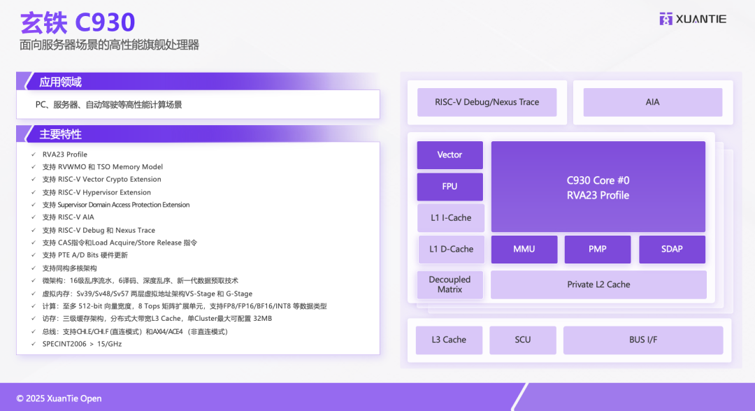
“Performance reaches the level of Arm’s X1 and N2,” which should refer to Cortex-X1 and Neoverse N2. The C930 is a CPU IP aimed at commercial server scenarios, “one of the industry’s most comprehensive and powerful IPs supporting the new RISC-V standard.” “This marks that RISC-V has reached a high level in the application processor field.”
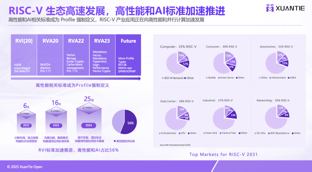
Not only Xuantie, but the RISC-V International Foundation’s instruction set configuration standard, the RVA23 Profile, has already mandated support for virtualization, vector computing, and matrix extensions to adapt to high-performance computing scenarios. In fact, before 2023, high-performance and AI-related projects accounted for 56% of the relevant standards. Therefore, RISC-V has long regarded high performance and AI as important development directions.
Sheng Fangwei shared data indicating that by 2031, RISC-V is expected to capture 30% of the market share across all major applications—statistics also include contemporary mainstream instruction sets like ARM and x86, as shown in the following figure:
From Xuantie’s current actions, we can further understand the development of the RISC-V ecosystem: its level and height of ecosystem construction have exceeded our expectations. Based on Sheng Fangwei’s speech, here are some representative events listed:
(1) Xuantie’s Senior Technical Expert Zhao Siqi was elected as the chair of the AME (Attached Matrix Extension) TG, promoting the evolution and standardization of Matrix technology—this is beneficial for exploring instruction directions that accelerate AI;
(2) In terms of AI acceleration, Xuantie has made Vector instruction extensions, AI Dot Turbo extensions (to accelerate dot product calculations), Vector SFU extensions (to meet the needs of large model development), and AME (Attached Matrix Extension) extensions;
(3) Xuantie has invested considerable effort in RISC-V virtualization software and hardware technology—Sheng Fangwei stated that based on the development foundation of Arm/x86 virtualization, RISC-V has quickly formed a complete and efficient virtualization mechanism, fully compatible with RISC-V H extensions; in the process of promoting virtualization technology, “we participated in the formulation and became contributors to the RISC-V IOMMU architecture specifications, and proposed GIPC for the RISC-V Scalable model;”
(4) The speech mentioned support for the “new 32-bit” compatibility, targeting 32-bit applications, Xuantie collaborated with PLCT Laboratory to jointly release a “new 32-bit” product-level open-source tool that runs 32-bit programs on 64-bit hardware; it is said to be based on the EF_RISCV_N32 structure, “which can utilize ILP32 to improve cache and memory efficiency while using RV64* ISA instructions to enhance performance”—those interested can check out Xuantie’s corresponding technology;
Other related autonomous extension interfaces, security, interconnect (multi-core interconnect scheduling), as well as specific IP products, design platforms, and development toolchains will not be elaborated here; we believe the above items are sufficient to showcase the high-level and rapid ecosystem construction status of RISC-V. Currently, Xuantie’s RISC-V IP licensing exceeds 800, with nearly 600 customers and cumulative chip shipments exceeding 4.5 billion units.
Another company that emphasized RISC-V at the forum was Canxin Semiconductor, highlighting its RISC-V chip customization turn-key solutions—this perfectly aligns with the main theme of the RISC-V era.
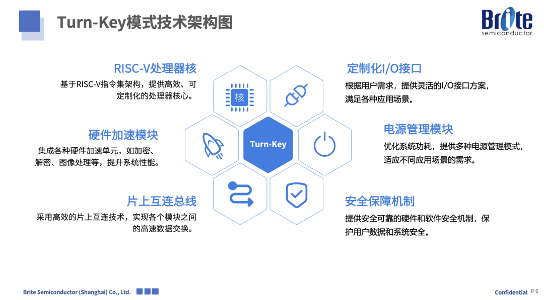
Yang Kai introduced that Canxin can provide efficient customized cores based on RISC-V; it can integrate various acceleration units—such as encryption/decryption, image processing, etc.; paired with efficient online interconnect technology, enabling high-speed data exchange between modules; flexibly providing IO interface solutions as needed; optimizing the power management module to reduce system power consumption; and providing security mechanisms to ensure data and system security… ultimately forming a complete turn-key model.
In fact, Canxin’s ability to provide such service models is also based on the open-source characteristics of the RISC-V instruction set, allowing for flexible configuration and customization to meet different scenario needs. Yang Kai listed customized solutions for AIoT edge chips, including those that meet low-power voice recognition and image processing needs, RISC-V dual-core with neural network accelerator combinations, and customized solutions for industrial control MCUs—meeting functional safety certification requirements, etc.; as well as examples of cases already achieved by Canxin, such as RISC-V-based communication ASIC customized chips and industrial control ASIC customized chips.
These also illustrate the prosperity of the RISC-V ecosystem, with Canxin being one of its ecosystem builders.
ARM Ecosystem: New A320 with NPU IP
ARM and Arm Technology are also not to be outdone in the AI era: when we look back from Armv7 to the latest Armv9.2, it is not difficult to see the advancements ARM has made at the instruction set level. Armv7-A introduced the well-known NEON; by Armv8.0-A, further extensions were made, “beginning to support 32 128-bit registers, allowing multiple multiply-accumulate operations to be performed in parallel”; Armv8.2-A NEON added support for FP16 and 8-bit dot product operations; and Armv9.2-A SVE2 introduced BF16 and matrix multiplication instruction support.
Not to mention the evolution from Trustzone to EL2, S-EL2, and more advanced security features such as PAC (Pointer Authentication Code)/BTI (Branch Target Identification)/MTE (Memory Tagging Extension) that enhance security…
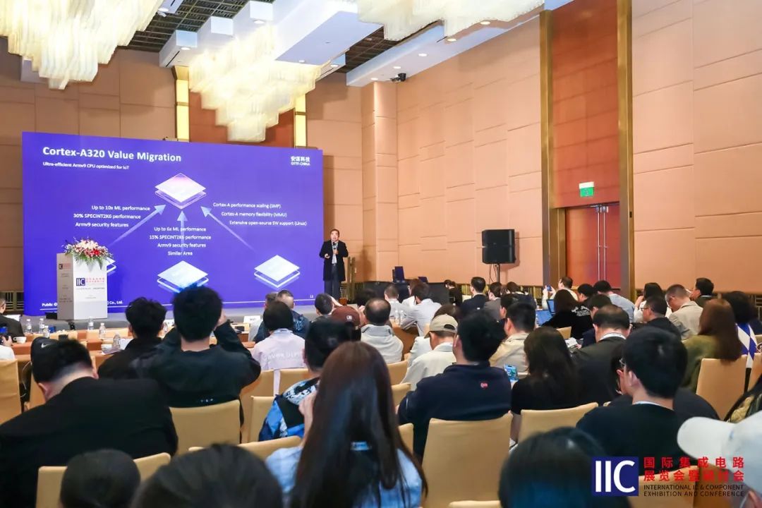
At the forum, Mao Weiyang mainly introduced products based on Armv9, including the Cortex-A320 and NPU IPs such as Ethos-U85 and Zhouyi. The Cortex-A320 is currently Arm’s major IP for edge applications, although its naming seems closer to the A520 used in mobile phones, Arm positions it for users of Cortex-M85, Cortex-A53, and Cortex-A35 who seek further DSP/ML performance.
For users of the Cortex-M series, Mao stated that the Cortex-A series offers a richer development environment and resources. “The A series supports complex operating systems like Linux and Android, can expand memory space, and better meets the AI computational power needs at the edge.” Therefore, upgrading from A35 to A320 results in a 10x increase in ML performance (mainly due to the introduction of SVE2), and a 30% increase in CPU’s SPECint2K6 performance; conversely, for A53 to A320, these values are 6x and 15%, and both have similar areas; compared to M85, the A series emphasizes performance improvements, MMU, and support for complex operating systems.
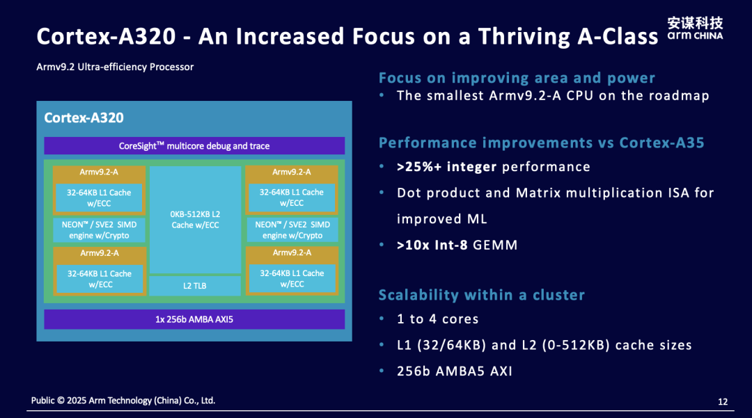
The Cortex-A320 is currently the smallest processor in the Armv9 architecture, boasting an excellent energy efficiency ratio. At the same time, it also introduces the security features of the Armv9 Cortex-A series, along with a significant increase in ML performance, and can be extended and generalized for different markets—even allowing “IoT to enjoy the rich software ecosystem of mobile phones.”
Details regarding the specific upgrade points of the Cortex-A320 microarchitecture, Armv9 security features, and AI computing enhancements, including the AI ecosystem with Arm Kleidi, will not be elaborated here—Arm’s official website should provide detailed explanations. In summary, the value of the Cortex-A320 encompasses (1) enhanced security features; (2) a broader software ecosystem; (3) significantly improved ML performance, aligning with the demands of the edge AI era—of course, there are also performance improvements compared to products like M85/A35, as well as support for expanded memory space.
In addition to CPU IPs, we must mention the NPU IPs from Arm and Arm Technology. When the edge faces higher computational power demands, relying solely on CPU and extended instructions for acceleration is clearly insufficient—especially for larger models with more parameters. Arm’s solution is that for light AI (~4TOPS), one can consider NPU like Ethos-U85.
The Ethos-U85 was originally an AI accelerator aimed at the embedded field, and the previously recommended pairing was Cortex M55/M85 + Ethos-U85. Now, Ethos-U85 can also be paired with Cortex-A320, “achieving close integration.” At a frequency of 1GHz, the U85 provides approximately 4TOPS of computational power.
When higher computational power is needed, one can also consider Arm Technology’s Zhouyi—Mao Weiyang specifically mentioned that “the next generation of NPU IP will be unveiled soon”—from the PPT, the new IP supports INT4/INT8/INT16/FP16 data formats; supports W4A16 hardware acceleration, where W4 refers to compressing neural network weights from conventional FP16 to INT4 storage, reducing memory usage and bandwidth requirements through quantization technology, while A16 maintains FP16 precision during computation to balance computational accuracy and efficiency—this helps reduce memory usage and improve computational efficiency;
Additionally, there is “special computation DSA acceleration,” which achieves dedicated acceleration to address the trend of increasing context length in the future, also enhancing the energy efficiency ratio for specific loads; especially optimized for Softmax and Layernorm; and continuous software investment to provide ongoing development of operator libraries, etc…
Furthermore, information regarding the upcoming NPU IP includes multi-task QoS management, a flexible IP licensing model that adapts to different customer characteristics and deep customization needs; and basic operations compatible with mainstream large models like DeepSeek, Tongyi Qianwen, and Llama. “We will release this product later, please stay tuned.”
More Accelerators and Peripheral IPs in the AI Era
Since the AI era emphasizes customization needs for different scenarios, the diversity of supporting IPs for the edge market is likely to continue until AI technology truly matures. Therefore, GPU IPs that can perform both graphics rendering and AI acceleration will inevitably hold a place in the market. Imagination, a regular at IIC, emphasized the AI computing power of its latest D series GPU at this forum.
Imagination’s efforts in the edge and endpoint AI fields should be based on its historical achievements in the mobile and automotive markets. Additionally, the company’s GPU IP is applied in various markets, including televisions, set-top boxes, wearable devices, and industrial fields. Sun Qianzhe, Application Engineering Manager at Imagination China, stated that Imagination’s GPU technology is particularly suited to the needs of edge computing.
In her keynote speech, she mainly introduced the IMG D series DXTP and DXS. The DXTP “is designed for power-constrained devices, balancing graphics processing and AI computation acceleration.” From a graphics rendering perspective, in classic tests like GFXBench Manhattan and Aztec Ruins, IMG DXTP outperforms the DXT series by 11%-22%.
This is mainly because, compared to DXT, while the number of USC module units within a single SPU has decreased, the overall number of SPUs has increased, leading to more geometric processing hardware modules—optimizing the architecture has improved geometric throughput by 50%, thus enhancing overall graphics performance.
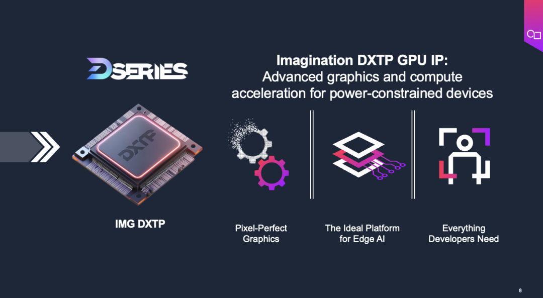
For edge AI, the DXTP “will accelerate smaller unit computational tasks, preventing task scheduling from becoming a bottleneck; it supports more data formats (FP16/FP32/INT8/DOT8); and increases local memory size.” Coupled with Imagination’s introduction of imgNN (neural network library), imgBLAS (linear algebra library), imgFFT (fast Fourier transform library) for OpenCL computing libraries, it also achieves a multiple increase in AI performance at the software level; along with optimizations in the LiteRT framework for the Android ecosystem, facilitating the deployment of AI applications on Android devices.
In addition to IMG DXTP, Sun Qianzhe also introduced the DXS series—this is a GPU IP primarily aimed at automotive applications. Besides the inherent advantages of the D series architecture in graphics rendering and AI computation (with a maximum extension of 9TFLOPS FP32 and 36TOPS INT8 computing power), DXS emphasizes its distributed safety mechanisms—achieving ASIL-B safety level at a relatively low cost.
Sun Qianzhe stated that typically, multi-core safety solutions run the same load on different cores or repeat the load on a single core to achieve error detection. “Such solutions may lose area or performance.” However, IMG DXS “inserts safety detection opportunities during relatively idle states, thus achieving error detection with minimal area overhead without sacrificing performance.” “Inserting safety mechanisms into different hardware blocks, each safety mechanism handles a relatively small part.” “This distributed safety mechanism is beneficial for quickly locating issues when failures occur.”
Of course, for a complete chip system, in addition to the aforementioned CPU and GPU core IPs, more auxiliary IPs are needed. Zhang Tao mentioned in his speech that the technical characteristics of AI innovative products not only include powerful computing power but also large-capacity storage, integration of more IPs, and low-power designs required for edge AI. The types of IP provided by Ruicheng Semiconductor include analog IP, interface IP, RF IP, and storage IP. The value of these IPs can be seen as looking further (analog IP), connecting more stably (RF IP), computing faster (interface IP), and remembering more reliably (storage IP).
For example, analog IP can achieve high-precision signal conversion, allowing weak signals to be amplified more accurately, PVT sensors for monitoring AI chip operating environment parameters, and high-performance low-power clocks are the “pulse of reliable CPU operation”; while interface IP, such as ultra-high-speed SerDes, “breaks the transmission bottleneck of data torrents”; RF IP ensures “always online in complex environments” under multi-band compatibility; and storage IP covers various NVM storage products, including AEC-Q100 Grade0 automotive-grade MTP…
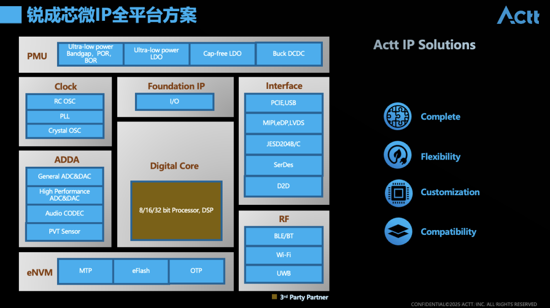
The above SoC product block diagram provides an overview of Ruicheng Semiconductor’s IP full-platform solutions. Notably, Zhang Tao specifically mentioned, “We provide overall IC design for customers—traditional IC design companies design chips conventionally, but now, as applications become more widespread, many application companies also want to customize chips that meet their application characteristics,” which is also Ruicheng Semiconductor’s target customers—this itself aligns with the trend of chip design in the AI era to meet specific application needs across more scenarios.
Chip Design is Fully AI-Driven
Interestingly, Cadence was also present at the conference—intuitively, Cadence, as a typical EDA company, is a backbone of the AI chip design era. However, Cai Zhun, Director of Technical Support at Cadence’s Customer Achievement Department, explained that Cadence’s full-stack “efficiency enhancement solution” essentially makes Cadence’s current strategy and solutions a living example of AI application, or that Cadence itself is a beneficiary of AI technology and the best portrayal of AI technology application. Therefore, we place Cadence at the end of this article for discussion.
Cai Zhun mentioned the limitations of traditional design processes, including reliance on engineers’ personal experience for optimization methods, manual parameter tuning, local performance optimization, and long simulation verification iteration cycles; the tool processes are not automated enough, and each step is relatively independent, “the entire process requires multiple data exchanges, including between tools and between people, affecting team productivity”; and chip, packaging, and system design, different stages of chip design are difficult to parallel, with low collaboration levels, and early issues are not easily discovered, increasing the likelihood of rework later.
The demands of modern chip system design require optimization in all three directions mentioned above. This includes optimizing methods, with EDA tools becoming intelligent, replacing manual intervention—achieving comprehensive performance optimization and shortening target realization cycles; design processes need to be automated, with seamless connections between each step—ultimately improving per capita productivity to meet human resource demands; and in terms of collaborative cooperation, cross-domain collaborative design is required, with analysis and verification moving forward—this way, risks can be identified early, reducing rework and accelerating product launch.
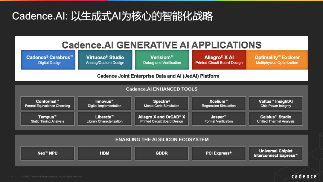
Cadence’s so-called “full-stack efficiency enhancement solution” emphasizes “automation,” “intelligence,” and “forward movement,” corresponding to the three points mentioned above. From a high-level abstract perspective, under the guidance of LLM AI strategies, in addition to providing big data and AI platforms to customers at the bottom level, the middle layer leverages Cadence’s strengths in digital simulation, verification, and other fields to provide AI optimization solutions, while the top layer, Cadence Copilot, uses LLM and various foundational models to help engineers improve efficiency. However, this was not the focus of Cai Zhun’s discussion this time.
Specifically, how Cadence’s tools and platforms apply AI technology to significantly speed up efficiency is limited by space, so a simple summary is made: Cai Zhun elaborated on (1) how different tools, including front-end design Verisium, back-end design Cerebrus, simulation design Virtuoso Studio, PCB design Allegro X AI, and multi-physical field simulation Optimality Explorer, utilize AI technology to achieve efficiency improvements; (2) simultaneously achieving multi-step automatic alignment and closed-loop optimization through process automation to enhance team productivity (for example, Smart Hierarchical Flow for automated hierarchical design processes, Certus Closure Solution); (3) and moving some of the later processes forward—such as RTL performance exploration, timing constraint verification, voltage drop and thermal analysis, etc…
Cai Zhun summarized the logic of these three components as (1) building on intelligence to promote the integration of EDA and AI across all fields, accelerating target realization; (2) bridging automation to connect the design process, promoting seamless connections between tools; (3) and moving forward to create a multi-domain collaborative platform, reducing management risks. However, discussing this theory feels somewhat dry; interested readers can explore how Cadence specifically practices this entire logic, as the details will be much more interesting.
Finally, we conclude with Mao Weiyang’s statement that AI is giving rise to “new species.” “With the development of edge AI, we also look forward to the emergence of more new product forms: this year, manufacturers have already released AI glasses, and earphone products seem to be considering integration with large models—achieving functions like translation at the edge, and smartwatches may also increasingly incorporate cameras for better scene understanding…” Mao said.
“There will be more and more new devices and new species emerging.” This presents a brand new development opportunity for the entire electronics industry, which is why some say that AI will far exceed the impact of smartphones on humanity. This is likely no longer an empty statement and is just around the corner.
Hot Articles
2025 China Fabless100 3+10 Category Top10 Rankings
2025-03-27

2025 China Fabless 100 Listed Company Rankings (Beta Version) Released!
2025-03-25
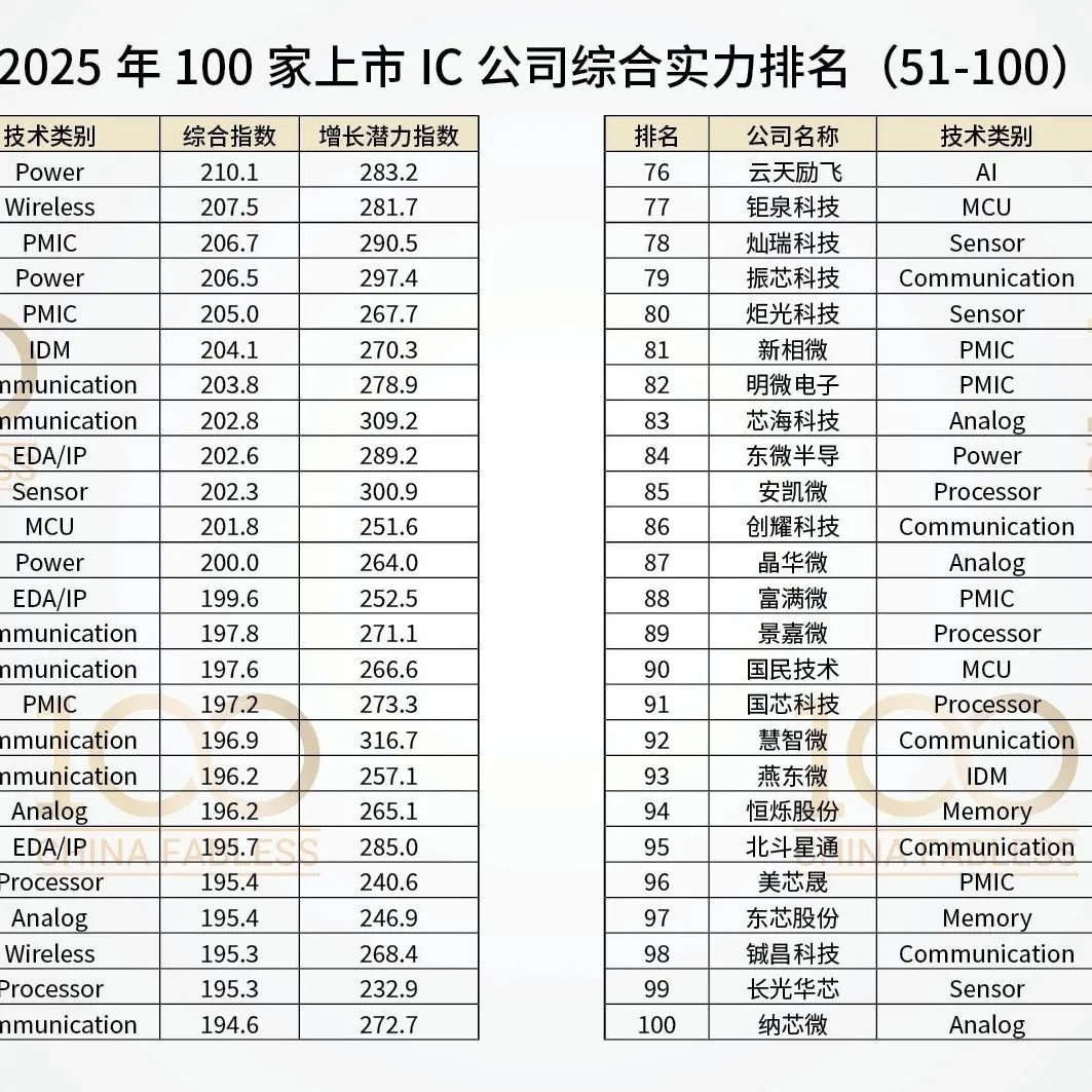
Model Open Source: How is the China Fabless 100 Ranking Calculated?
2025-03-25
Under Trump’s “Reciprocal Tariffs,” Auto Manufacturers Accelerate Transporting Core Components to the U.S.
2025-03-26

$390 Million Smuggling Case! The U.S. Pressures Singapore and Malaysia to Strictly Investigate AI Chip Flow Issues
2025-03-25