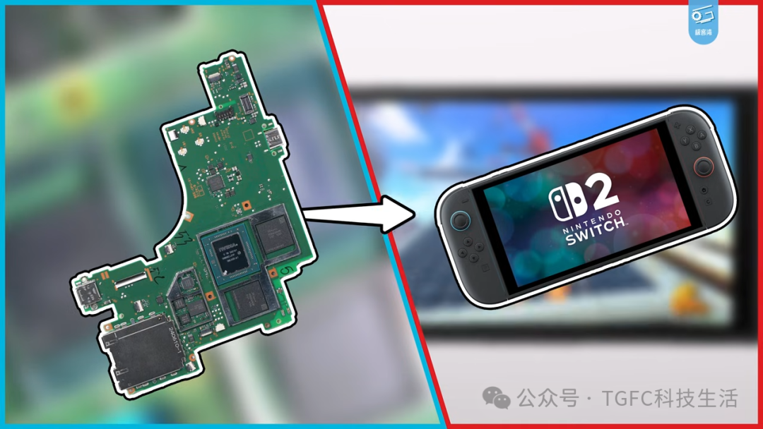
Nintendo’s culture of secrecy has always been tight, even bugs in “Zelda” are hidden like treasures. But this time, the mainboard and SoC of the Switch 2 have surprisingly been unearthed by players from a certain marketplace?!
And it’s not just images or concept art; it’s a physical mainboard + teardown video + GPU analysis triple whammy, with even the chip area measured!
📦 This is not an official teaser; this is a “black market premiere”. The whole situation is like:
Switch 2 hasn’t been released yet, and Geekerwan has already taken it apart.
💻 Switch 2 SoC Exposed: Area Explodes, Surpassing RTX 3050 Ti?
According to a teardown video by Bilibili tech creator Geekerwan, he obtained a suspected Switch 2 mainboard and chip (SoC) and conducted an in-depth analysis.
The most explosive data is as follows:
-
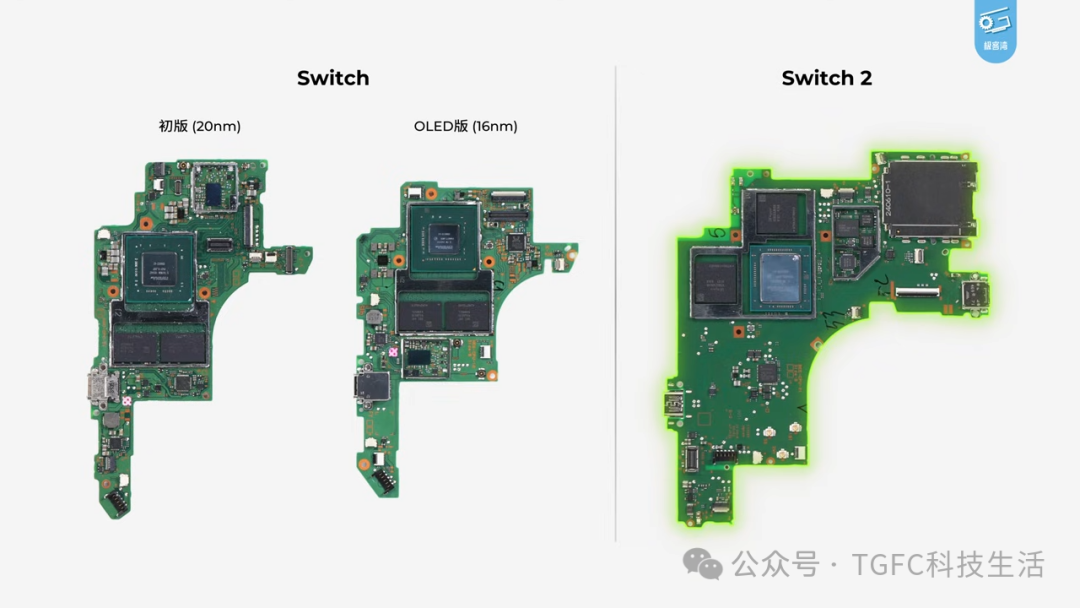
💥 Chip Area: 207 square millimeters
-
👉 The previous generation Switch’s Tegra X1 chip area was: 118 mm²
-
🧠 Larger than the mobile version of RTX 3050 Ti!
🤯 A handheld chip area surpassing mid-range laptop graphics cards? Is it going to directly solder the graphics card into the controller?
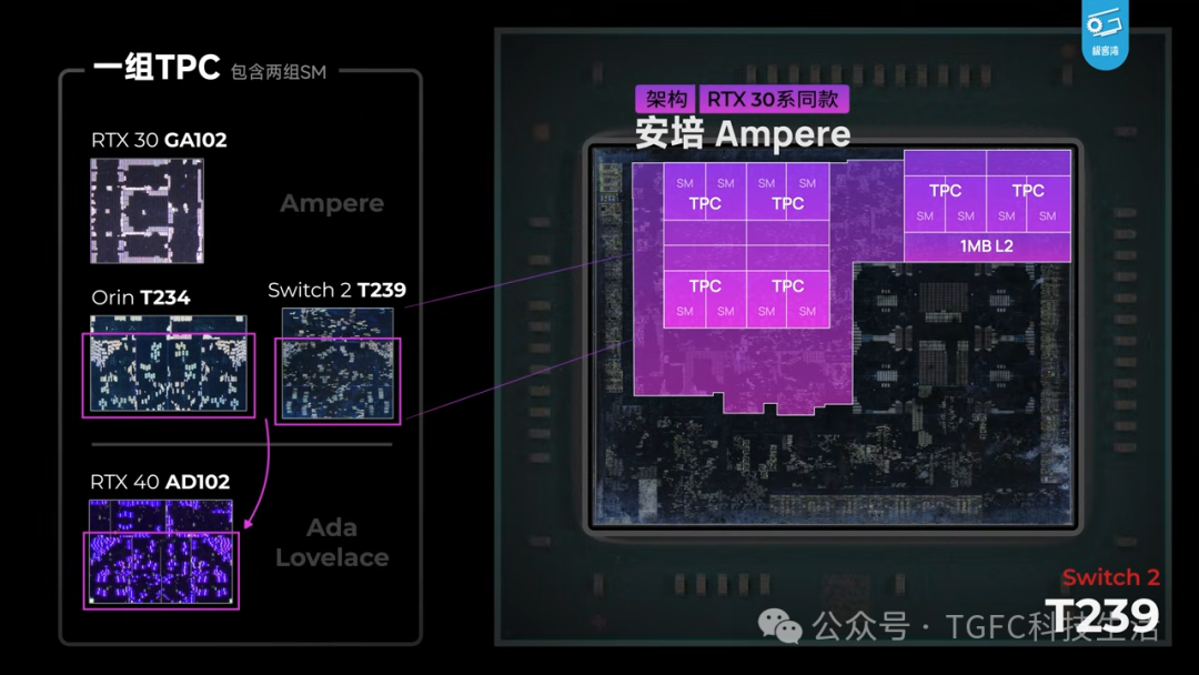
🧬 Is it “Ampere” or “Ada”? This GPU has quite a personality.
Geekerwan stated that this GPU is classified as Ampere architecture, but its layout is closer to Ada Lovelace architecture (which is related to the RTX 40 series).
✅ Core configuration is as follows:
-
6 TPCs (Texture Processing Clusters)
-
Each TPC contains 2 SMs (Streaming Multiprocessors)
-
In total, 1536 CUDA cores
This specification is already at the level of mid-range PC graphics cards. Let me emphasize again, this is a gaming handheld, not your desktop RTX + water-cooled tower defense machine.
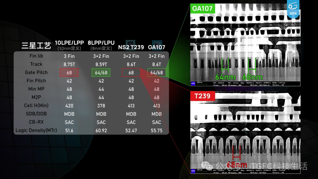
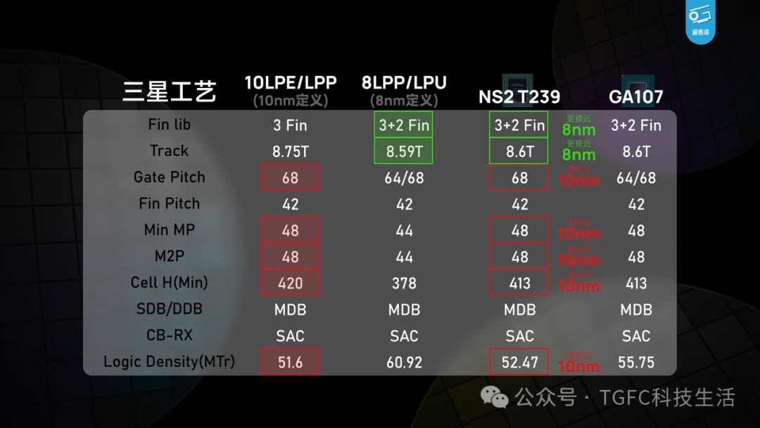
🤔 Process Technology: Neither 8nm nor 10nm? Samsung’s “mysterious hybrid”.
The chip of the Switch 2 is marked with “Tape-out time: 2021”, which also explains why everyone says “Switch 2 has actually been built for a long time, just waiting for a good day to release”.
As for the process technology?
-
🧪 On the surface, it is 8nm
-
🔍 In practice, it looks more like Samsung’s 10nm derivative version
To put it bluntly, this chip uses a “looks like 8nm, but fundamentally still 10nm” hybrid process. The impact on players is:
Heat control may not be as stable as TSMC, but it is cheaper and can be mass-produced faster, making it quite reasonable for Nintendo to use it.
🤯 Comment Section Controversy: Can the performance really hold up?
Now the question arises, although the parameters of this SoC are explosive, whether it can truly deliver unbeatable performance, no one can guarantee. Why?
Because the performance of a handheld depends not only on the cores but also on:
-
Can the cooling handle these CUDA cores🔥
-
Can the battery support this “laptop-level” chip🔋
-
Can game development make good use of this hardware🧩
-
Is Nintendo willing to push it to the max, not lock the frequency🕹️
🗣️ So, what do you think about this?
🔥View A: This is undoubtedly a next-gen handheld! It beats the Steam Deck!🔥View B: No matter how impressive the paper specs are, Nintendo will still lock frame rates and quality🔥View C: Forget about performance, I just want to play high-definition Zelda🔥View D: Do you think Nintendo is a performance player? They just want Mario to run smoothly
🕵️ Geekerwan has hit the jackpot this time: tearing down a Switch 2, clarifying half of the chip world
To add, the reason Geekerwan’s video went viral is that the content is not only “daring to speak” but also “thoroughly explained”.
The device he obtained is said to be from a “early bird console” on a certain marketplace, an internal testing machine that was leaked early—although this point has not been officially confirmed yet, the credibility is quite high based on the mainboard design, chip structure, and packaging method.
🎯 The key point is, Nintendo has been denying the Switch 2, yet before you officially speak, people have already been able to lithograph your chip.
🎮 How powerful is the Switch 2? The real machine will tell.
From chip area to architecture design, from hybrid process to GPU configuration, this time the Switch 2 is no longer a toy, but a handheld beast that can seriously compete with “half a laptop”.
But the questions remain:
-
🧨Will it lock performance?
-
🧨When will the official announcement be made?
-
🧨Will this generation support ray tracing? Genshin Impact at 120fps? Or will it still be locked at 30fps?
This is the charm of Nintendo— you never know if they are playing a performance game or pulling a sentimental trick.
#Nintendo #Switch2
Previous Recommendations
Switch 2 not suitable for Unreal 5? Don’t rush to criticize, it might just be an “incomplete version”
2025-05-06
Nintendo sues accessory manufacturers just because they “leaked” Switch 2? Netizens: The legal department is flexing again!
2025-05-05
Switch 2 plays “Street Fighter 6” from 540p directly to 1080p?! DLSS: Yes, I rely entirely on AI “upscaling”!
2025-04-26
If you like this public account, please help by liking, sharing, viewing, and rewarding! Thank you all!