I have a demo board with an integrated MOSFET Buck power supply. Although the circuit is simple, the layout is quite textbook-like. Here are some key design points of this circuit:
1. Phase Plane
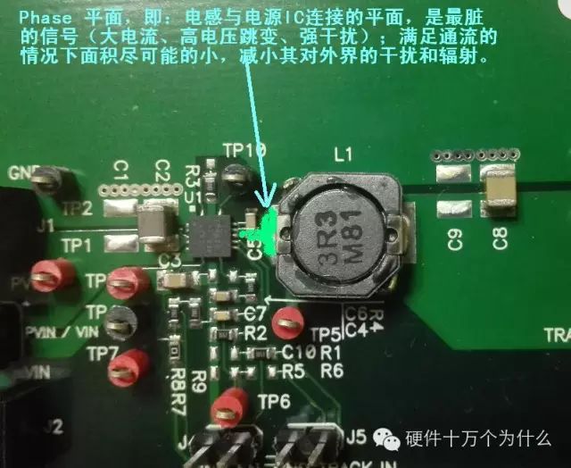
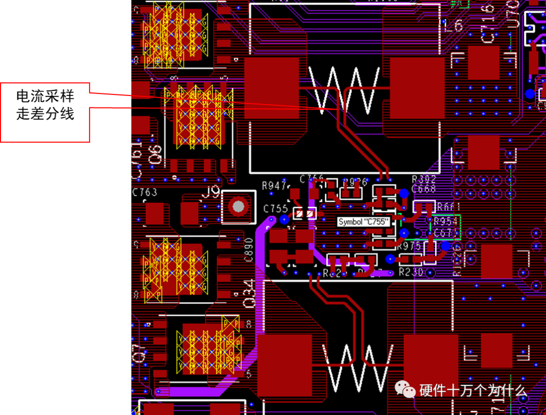
The phase plane, which is the plane connecting the inductor and the power IC, is the dirtiest signal (high current, high voltage transitions, strong interference); the area should be minimized under the condition of current flow to reduce its interference and radiation to the outside.
2. Loop Compensation and Small Signals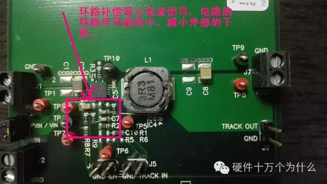 For small current signals like loop compensation, the circuit loop should be as small as possible, reducing the area to decrease the external interference magnetic flux and the degree of interference, ensuring the stability and signal-to-noise ratio.
Summary: Strong interference signals (Phase plane) are like a toilet (dirty signals), while small signal circuits (loop compensation) are like a kitchen (signals that are easily interfered with).
In PCB design, the principle is to protect the kitchen from interference from the toilet; this applies to power supply design as well as other circuit designs.
In one case with this chip, the EN pin was placed too close to the Phase pin during design; EN was easily interfered with by Phase, and noise from the switching frequency could be tested on EN. During PCB design, it is necessary to reduce the parallel routing of these two signals and increase the spacing as much as possible; otherwise, there is a probabilistic occurrence of EN being interfered with, leading to unintended power shutdown. (Like the smell from the toilet wafting into the kitchen).
At the same time, we can also add a pull-down capacitor to ground on the EN pin for filtering.
Interference from other pins and networks, with EN at a minimum of 1.14V, can lead to unintended power shutdown.
1. Control Interference Sources (Dirty Signals) through PCB Design
During the design process, we must first identify the source of interference and distinguish whether it is current interference or voltage interference. If it is current interference, we need to minimize the area of the current loop; if it is voltage interference, we need to reduce the copper area of the interference voltage network points.
In a Buck architecture DC/DC converter, there are two main loops where current changes dramatically:
When the upper bridge MOSFET Q1 is turned on, current flows from the power supply through Q1 and L1 to the output capacitor and load, then returns to the power input through the ground. During this process, the alternating components of the current will flow through the input and output capacitors. The current path mentioned here is shown by the red line in the diagram, labeled as I1.
When Q1 is turned off, the inductor current will continue to flow in the original direction, while the synchronous rectifier switch MOSFET Q2 will turn on at this time, and the current will flow through Q2, L1, and the output capacitor, returning to Q2 through the ground. Its loop is shown by the blue line in Figure 2, labeled as I2.
Both currents I1 and I2 are discontinuous, meaning they have steep rising and falling edges during switching, which results in a very high current change rate dI/dt, thus containing many high-frequency components.
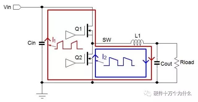
Current loops in the BUCK converter
In the loops described above, current loops I1 and I2 share the path from the switching node à inductor à output capacitor à ground à source of Q2. When combined, I1 and I2 form a relatively smooth, continuous sawtooth waveform, as there are no edges with a high current change rate dI/dt, resulting in fewer high-frequency components.
From the perspective of electromagnetic radiation, the shaded area A1 in the figure contains the loop with a high current change rate dI/dt, which will generate the most high-frequency components, thus being a critical part to consider in the EMI design of the Buck converter. The current change rate dI/dt in area A2 is not as high as in area A1, resulting in less high-frequency noise.
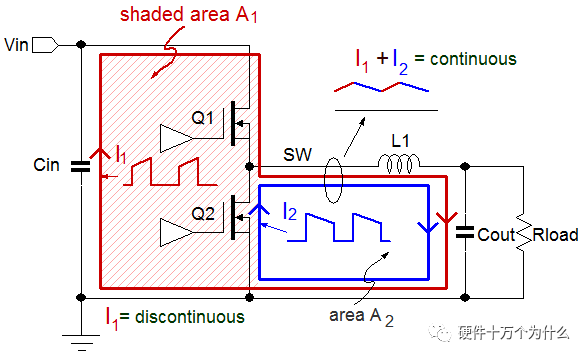
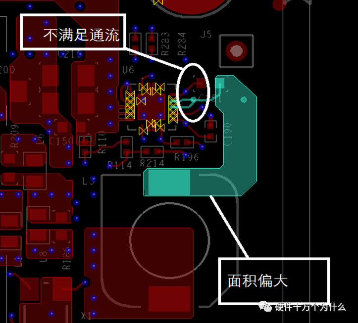
When designing the PCB layout for the Buck converter, the area of A1 should be designed to be as small as possible.
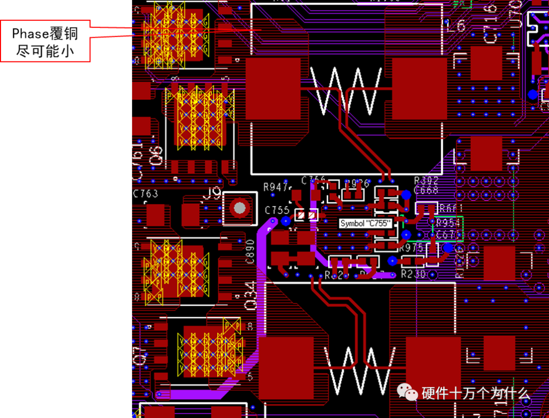
There are also high-frequency switching nodes (SW node) in the BUCK circuit, where dv/dt generates electric fields and radiation, and the common-mode current generated also plays an important role in conducted testing. High-frequency switching nodes are often related to radiation, especially in monopole antenna tests and biconical antenna tests, where the near-field electric field generated by high-frequency switching nodes can be directly received by the monopole antenna.
To suppress the dv/dt of high-frequency switching nodes, we can first reduce the area to decrease the near-field electric field strength. As shown in the figure, by reducing the copper area of SW, the electric field strength is significantly reduced. Similarly, in monopole testing, we can achieve this by reducing the copper area of SW or the size of the inductor. We have previously analyzed that inductors cannot maintain a stable potential, making them high-frequency switching nodes as well.
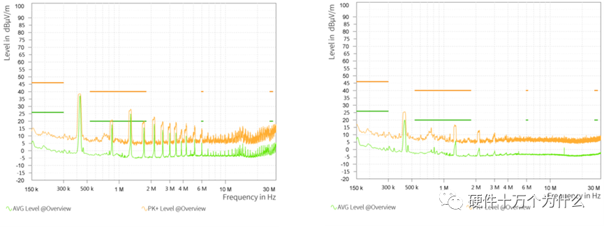
When power is limited, and the inductor size cannot be significantly reduced, shielded inductors can be used. Here, shielded inductors refer to inductors with a metal layer as a shielding layer that is grounded, not inductors with copper shielding integrated into the design. For example, the automotive-grade IHLE integrated electric field shielded inductor from VISHAY has a metal casing that needs to be grounded during use to provide a stable zero point, achieving electric field shielding effects.
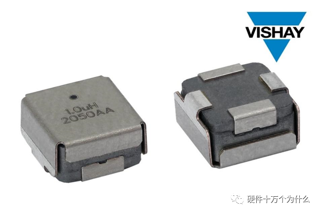
Measured monopole antenna tests (150K~30M) of shielded inductors show nearly 20dB of suppression effect after using shielded inductors. Of course, in practice, we can use metal enclosures to shield the SW node and the inductor.
We know that common-mode currents exist in conducted and radiated testing, especially in radiated testing, where they play an important role and need to be suppressed. As shown in the figure, analyzing the path of common-mode currents, we can suppress common-mode currents in three ways.
-
1. Reduce the switching area and inductor size of dv/dt to weaken the electric field strength.
-
2. Shield the SW node and inductor to provide a zero level for dv/dt noise, reducing coupling capacitance.
-
3. Add common-mode inductors at the input to increase the impedance of the common-mode loop.
2. Protect Sensitive Signals
For signals that are easily interfered with, we should reduce the probability and intensity of external interference through routing separation and minimizing loops.
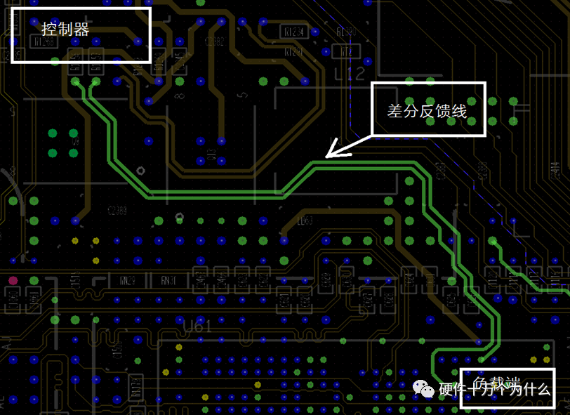
Feedback differential routing for power supply voltage at a distance
Voltage detection is divided into feedback detection and feedback detection. Generally, small current power supplies use near-end feedback, as shown in the circuit for detection. The voltage divider resistors and feedback lines are placed close to the power output (output capacitor) and can be single-ended signal feedback.
Generally, large current power supplies use far-end feedback, as shown in the circuit for detection. (If there are voltage divider resistors, they should be placed close to the controller.) The main purpose of the differential pair is to suppress common-mode interference, so there are no strict requirements on the length of the differential pair.
Minimize the area of loop compensation
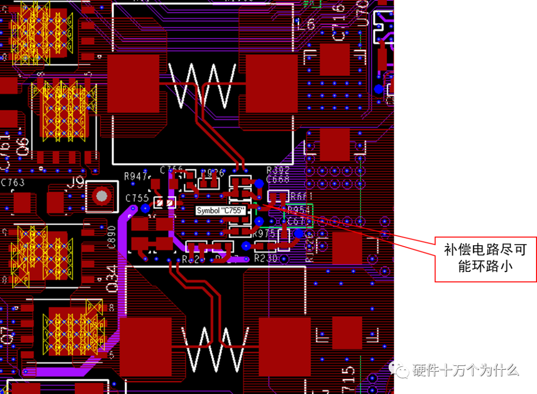
Similarly, for other sensitive signals, we hope to reduce their interference from dirty signals by minimizing area, reducing loops, and increasing distance from dirty signals.
Previous Series Content:
My process of improving understanding of PCB design【1】Driven by Interest
My process of improving understanding of PCB design【2】Should Hardware Engineers Draw PCBs Themselves?
My process of improving understanding of PCB design【3】How Long Should PCB Traces Be?
My process of improving understanding of PCB design【4】How Wide Should PCB Traces Be?
My process of improving understanding of PCB design【5】Inner Layers of PCB
My process of improving understanding of PCB design【6】Via Holes
My process of improving understanding of PCB design【7】Can PCB Traces Have Sharp Angles and Right Angles?
My process of improving understanding of PCB design【8】Should Copper Islands Be Retained? (PCB Islands)
My process of improving understanding of PCB design【9】Can Vias Be Placed on Pads?
My process of improving understanding of PCB design【10】What Material is FR4?
My process of improving understanding of PCB design【11】Solder Mask, Why is Green Most Common?
My process of improving understanding of PCB design【12】Steel Mesh
My process of improving understanding of PCB design【13】Pre-layout
My process of improving understanding of PCB design【14】Principles of PCB Layout and Routing
My process of improving understanding of PCB design【15】Cross-segment Routing
My process of improving understanding of PCB design【16】Signal Reflection
Recommended Book: “100,000 Questions About Hardware (Development Process Edition)”
Scan the QR code to learn more about the book:

“Cadence High-Speed PCB Design” Book Purchase Full Refund Coupon Activity