Main reference materials:
Bilibili @ Jiangxie Technology
STM32 Beginner Tutorial – 2023 Edition Detailed Explanation with Chinese Subtitles
Development materials download link: https://pan.baidu.com/s/1h_UjuQKDX9IpP-U1Effbsw?pwd=dspb
Microcontroller kit: STM32F103C8T6 development board microcontroller C6T6 core board experimental board minimum system board kit
Introduction to I2C Peripherals
- • The STM32 integrates hardware I2C transceiver circuits, which can automatically execute clock generation, start/stop condition generation, acknowledgment bit transmission/reception, and data transmission/reception functions, reducing the burden on the CPU.
- • Supports multi-master model
- • Supports 7-bit/10-bit addressing modes
- • Supports different communication speeds: standard speed (up to 100KHz), fast (up to 400KHz)
- • Supports DMA
- • Compatible with SMBus protocol
- • STM32F103C8T6 hardware I2C resources: I2C1, I2C2
I2C Block Diagram
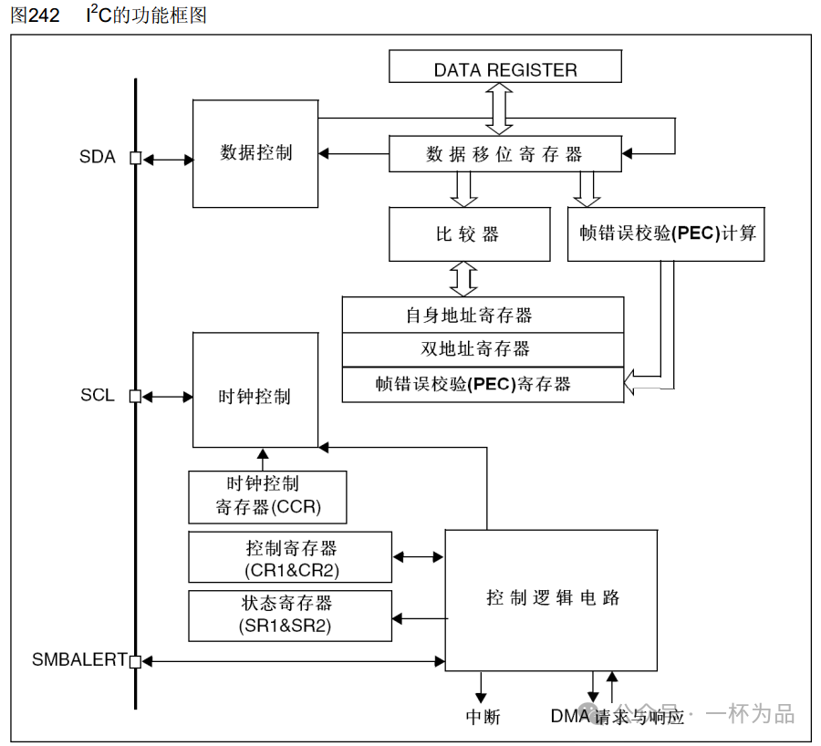
The communication pins SDA and SCL are on the left side of the I2C peripheral block diagram, and the specific GPIO pins used are listed in the pin definition table. SMBALERT is the pin used for SMBus. In the data control section, the core components for data transmission and reception are the Data Register (DR) and the Data Shift Register, with a process similar to serial communication. When sending data, a byte of data can be written into the DR, which directly transfers the data into the shift register when it is idle, setting the TXE flag. The shift register then shifts the data, allowing the DR to receive the next byte of data. When receiving data, the input data shifts from the pin to the shift register, and after a byte of data has been shifted, the data is transferred from the shift register to the DR, setting the RXNE flag, at which point the data can be read. The start condition, stop condition, and acknowledgment bits are all handled by the control circuit.
The comparator, self-address register, and dual-address register are used for communication when the STM32 acts as a slave. The self-address register stores the slave address of the STM32. When the STM32 is addressed as a slave, if the received address matches the self-address as determined by the comparator, the STM32 responds. The STM32 also supports responding to two slave addresses simultaneously, hence the dual-address register. The frame error check register and frame error check calculation automatically perform CRC checks for data validity verification. This experiment does not involve these functions. The clock control and control logic circuits for the SCL pin can be viewed as a black box, and the details of the principles do not need to be mastered at this time.
Basic Structure of I2C
The I2C structure required for this experiment is simplified as follows:
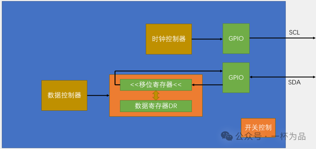
Master Sending
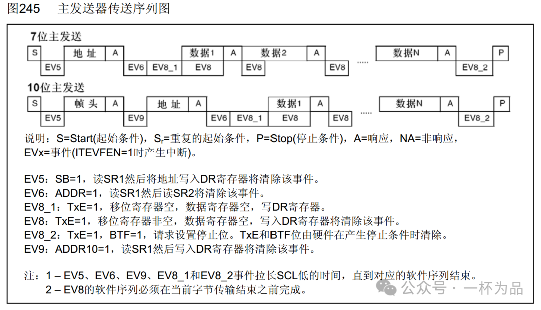
The above diagram shows the flowchart for master sending, focusing only on the 7-bit sending. EVx represents events triggered at different stages of communication, and there are corresponding functions in the library to check if EVx has occurred, which can be understood as major flags.
When sending, the START bit in the control register I2C_CR1 must be set to 1 to automatically generate the start condition. After detecting the start condition, the slave address can be written into the DR, which is automatically sent by the hardware circuit, followed by automatic acknowledgment reception and judgment. If there is no acknowledgment, the hardware sets the acknowledgment failure flag, which can request an interrupt. After addressing is complete, EV6 and EV8_1 are triggered in succession, at which point we need to write to the DR to send data. When the shift register sends data, the EV8 event occurs, and during the EV8 event, data can continue to be written to the DR and the event cleared, so the end of EV8 in the diagram occurs at any time before the next data transmission. If the shift register has finished sending data and the DR still has no new data, it indicates the byte sending is complete, generating the EV8_2 event, which can automatically generate the stop condition by writing 1 to the STOP bit in I2C_CR1.
Master Receiving
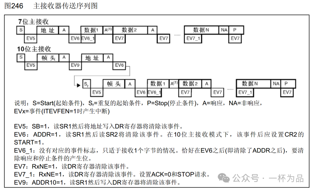
When receiving, set the START bit to 1 to generate the start condition, the EV5 event can write the address, the EV6 event indicates addressing is complete, and EV6_1 occurs when receiving the first byte of data. Before receiving each byte of data, the ACK must be configured in I2C_CR1, writing 0 for no acknowledgment and 1 for acknowledgment. EV7 occurs after the data is transferred from the shift register to the DR, at which point the data can be read and the event cleared. If no further data needs to be received, write 0 to ACK and set the STOP request in the last timing unit, which is the EV7_1 event.
Function Details
I2C_DeInit Function
Overview: Restores default configuration.
Parameter: I2C name
I2C1/2I2C_Init Function
Overview: Initializes I2C.
Parameter 1: I2C name
Parameter 2: Pointer to I2C_InitTypeDef structure
I2C_InitTypeDef Structure
Member I2C_Mode: Mode
I2C_Mode_I2C (I2C)
I2C_Mode_SMBusDevice (SMBus Device)
I2C_Mode_SMBusHost (SMBus Host)
Member I2C_ClockSpeed: Clock frequency, standard speed 0~100KHz, fast 100~400KHz.
Member I2C_DutyCycle: Clock duty cycle, fixed 1:1 for standard speed, fast can select the following parameters (low level: high level).
I2C_DutyCycle_16_9 (16:9)
I2C_DutyCycle_2 (2:1)
Since the I2C data line is strongly pulled down and weakly pulled up during communication, the SDA level requires a certain flip time to go from low to high, and in fast mode, the SCL low level time needs to be appropriately extended.
Member I2C_Ack: Acknowledgment bit configuration
I2C_Ack_Enable/DisableMember I2C_AcknowledgedAddress: Number of address bits for STM32 to respond as a slave
I2C_AcknowledgedAddress_10bit/7bitMember I2C_OwnAddress1: STM32’s own address as a slave
I2C_StructInit Function
Overview: Initializes I2C_InitTypeDef structure.
Parameter: Pointer to I2C_InitTypeDef structure
I2C_Cmd Function
Overview: Enables I2C.
Parameter 1: I2C name
Parameter 2: Enable/Disable
I2C_GenerateSTART Function
Overview: Generates start condition.
Parameter 1: I2C name
Parameter 2: Enable/Disable
I2C_GenerateSTOP Function
Overview: Generates stop condition.
Parameter 1: I2C name
Parameter 2: Enable/Disable
I2C_AcknowledgeConfig Function
Overview: Configures ACK bit.
Parameter 1: I2C name
Parameter 2: Enable/Disable
I2C_SendData Function
Overview: Writes data to DR.
Parameter 1: I2C name
Parameter 2: Data
I2C_ReceiveData Function
Overview: Reads data from DR.
Parameter: I2C name
I2C_Send7bitAddress Function
Overview: Sends 7-bit address.
Parameter 1: I2C name
Parameter 2: Address
Parameter 3: Read/Write mode
I2C_Direction_Transmitter (Write)
I2C_Direction_Receiver (Read)
I2C_CheckEvent Function
Overview: Detects events.
Parameter 1: I2C name
Parameter 2: Event
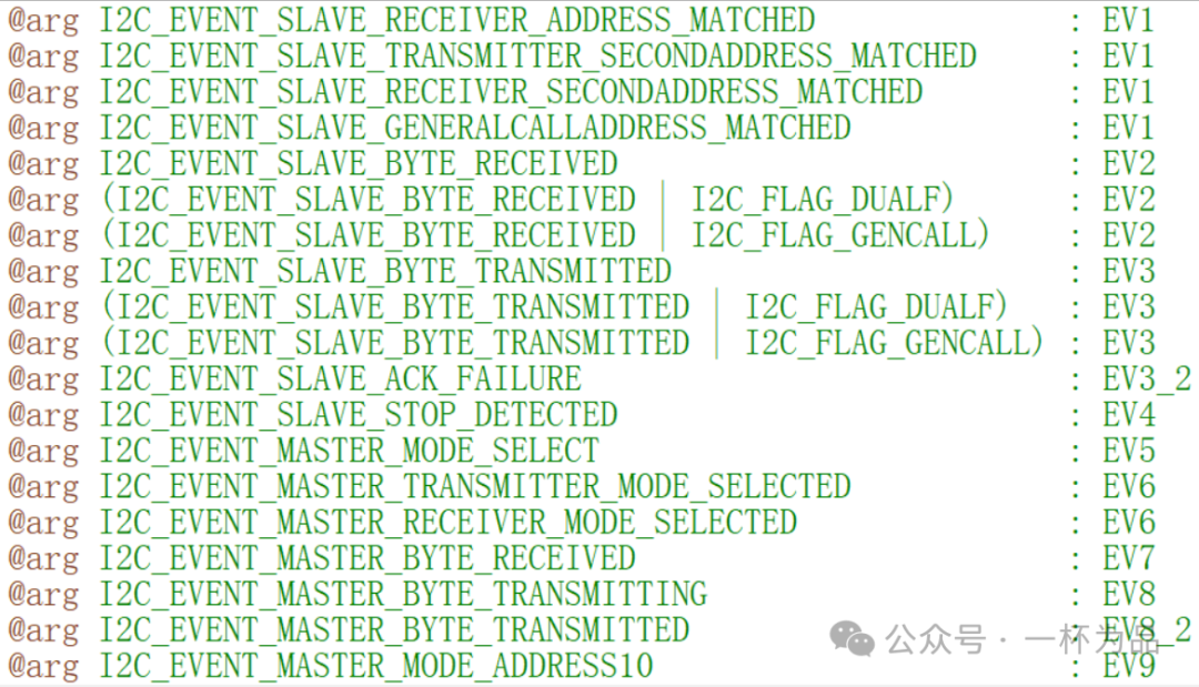
Return Value
SUCCESS, ERRORInterrupt Flag Functions
I2C_GetFlagStatus Function
I2C_ClearFlag Function
Parameter 1: I2C name
Parameter 2: I2C flag
I2C_FLAG_TXE
I2C_FLAG_RXNE
Other flags not used for now
I2C_GetITStatus Function
I2C_ClearITPendingBit Function
Parameter 1: I2C name
Parameter 2: I2C interrupt source
Experiment 25 Hardware I2C Read/Write MPU6050
The wiring diagram is the same as Experiment 24, with pins PB10/11 corresponding to I2C2.
Delete the MyI2C driver from Experiment 24, and use the built-in library functions in the MPU6050 driver.
MPU6050 Driver
The header file remains unchanged, and the source file replaces all MyI2C functions in MPU6050 with library functions, with the original code kept as comments for reference.
MPU6050.c
#include "stm32f10x.h"
#include "MPU6050_Reg.h"

#define MPU6050_ADDRESS 0xD0

void MPU6050_WriteReg(uint8_t RegAddress, uint8_t Data)
{
//    MyI2C_Start();
//    MyI2C_SendByte(MPU6050_ADDRESS);
//    MyI2C_ReceiveAck();
//    MyI2C_SendByte(RegAddress);
//    MyI2C_ReceiveAck();
//    MyI2C_SendByte(Data);
//    MyI2C_ReceiveAck();
//    MyI2C_Stop();
    I2C_GenerateSTART(I2C2, ENABLE);
    //I2C functions only configure registers, their completion does not mean waveform transmission is complete, need to check corresponding events
    //Wait for EV5
    while(I2C_CheckEvent(I2C2,I2C_EVENT_MASTER_MODE_SELECT) != SUCCESS);
    //The function automatically adjusts the lowest bit of the address byte according to the transmission direction
    I2C_Send7bitAddress(I2C2, MPU6050_ADDRESS, I2C_Direction_Transmitter);
    //The acknowledgment bit is automatically handled by hardware, wait for EV6 (send mode)
    while(I2C_CheckEvent(I2C2,I2C_EVENT_MASTER_TRANSMITTER_MODE_SELECTED) != SUCCESS);
    I2C_SendData(I2C2, RegAddress);
    //Wait for EV8 during continuous sending
    while(I2C_CheckEvent(I2C2,I2C_EVENT_MASTER_BYTE_TRANSMITTING) != SUCCESS);
    I2C_SendData(I2C2, Data);
    //Wait for EV8_2 during the last send
    while(I2C_CheckEvent(I2C2,I2C_EVENT_MASTER_BYTE_TRANSMITTED) != SUCCESS);
    I2C_GenerateSTOP(I2C2, ENABLE);
}

uint8_t MPU6050_ReadReg(uint8_t RegAddress)
{
    uint8_t Data;
//    MyI2C_Start();
//    MyI2C_SendByte(MPU6050_ADDRESS);
//    MyI2C_ReceiveAck();
//    MyI2C_SendByte(RegAddress);
//    MyI2C_ReceiveAck();
//
//    MyI2C_Start();
//    MyI2C_SendByte(MPU6050_ADDRESS | 0x01);
//    MyI2C_ReceiveAck();
//    Data = MyI2C_ReceiveByte();
//    MyI2C_SendAck(1);
//    MyI2C_Stop();
    //The address sending part is reused from WriteReg function
    I2C_GenerateSTART(I2C2, ENABLE);
    while(I2C_CheckEvent(I2C2,I2C_EVENT_MASTER_MODE_SELECT) != SUCCESS);
    I2C_Send7bitAddress(I2C2, MPU6050_ADDRESS, I2C_Direction_Transmitter);
    while(I2C_CheckEvent(I2C2,I2C_EVENT_MASTER_TRANSMITTER_MODE_SELECTED) != SUCCESS);
    I2C_SendData(I2C2, RegAddress);
    //Since only one data is sent after the slave address, this EV8 is changed to EV8_2
    while(I2C_CheckEvent(I2C2,I2C_EVENT_MASTER_BYTE_TRANSMITTED) != SUCCESS);
    //Repeat start condition
    I2C_GenerateSTART(I2C2, ENABLE);
    //Wait for EV5
    while(I2C_CheckEvent(I2C2,I2C_EVENT_MASTER_MODE_SELECT) != SUCCESS);
    //Change direction to receive
    I2C_Send7bitAddress(I2C2, MPU6050_ADDRESS, I2C_Direction_Receiver);
    //Wait for EV6 (receive mode)
    while(I2C_CheckEvent(I2C2,I2C_EVENT_MASTER_RECEIVER_MODE_SELECTED) != SUCCESS);
    //Single byte (last byte) reception, ACK and stop conditions must be configured immediately after EV6, otherwise acknowledgment will be sent when data is received
    I2C_AcknowledgeConfig(I2C2, DISABLE);
    I2C_GenerateSTOP(I2C2, ENABLE);
    //Wait for EV7
    while(I2C_CheckEvent(I2C2,I2C_EVENT_MASTER_BYTE_RECEIVED) != SUCCESS);
    //Read DR
    Data = I2C_ReceiveData(I2C2);
    //Restore ACK configuration to default for multi-byte reception
    I2C_AcknowledgeConfig(I2C2, ENABLE);
    return Data;
}

void MPU6050_Init(void)
{
//    MyI2C_Init();
    RCC_APB1PeriphClockCmd(RCC_APB1Periph_I2C2, ENABLE);
    RCC_APB2PeriphClockCmd(RCC_APB2Periph_GPIOB, ENABLE);

    GPIO_InitTypeDef GPIO_InitStructure;
    //Open-drain output for multiplexing, peripherals use multiplexing, I2C protocol requires open-drain
    GPIO_InitStructure.GPIO_Mode = GPIO_Mode_AF_OD;
    GPIO_InitStructure.GPIO_Pin = GPIO_Pin_10 | GPIO_Pin_11;
    GPIO_InitStructure.GPIO_Speed = GPIO_Speed_50MHz;
    GPIO_Init(GPIOB, &GPIO_InitStructure);

    I2C_InitTypeDef I2C_InitStructure;
    //Initialize with default acknowledgment
    I2C_InitStructure.I2C_Ack = I2C_Ack_Enable;
    I2C_InitStructure.I2C_ClockSpeed = 50000;
    //Clock duty cycle is invalid at standard speed
    I2C_InitStructure.I2C_DutyCycle = I2C_DutyCycle_2;
    I2C_InitStructure.I2C_Mode = I2C_Mode_I2C;
    //Address can be arbitrary in non-slave mode
    I2C_InitStructure.I2C_AcknowledgedAddress = I2C_AcknowledgedAddress_7bit;
    I2C_InitStructure.I2C_OwnAddress1 = 0x00;
    I2C_Init(I2C2, &I2C_InitStructure);

    I2C_Cmd(I2C2, ENABLE);
    //I2C initialization complete

    MPU6050_WriteReg(MPU6050_PWR_MGMT_1, 0x01);
    MPU6050_WriteReg(MPU6050_PWR_MGMT_2, 0x00);
    MPU6050_WriteReg(MPU6050_SMPLRT_DIV, 0x09);
    MPU6050_WriteReg(MPU6050_CONFIG, 0x06);
    MPU6050_WriteReg(MPU6050_GYRO_CONFIG, 0x18);
    MPU6050_WriteReg(MPU6050_ACCEL_CONFIG, 0x18);
}

uint8_t MPU6050_GetID(void)
{
    return MPU6050_ReadReg(MPU6050_WHO_AM_I);
}

void MPU6050_GetData(int16_t *AccX, int16_t *AccY, int16_t *AccZ,
                    int16_t *GyroX, int16_t *GyroY, int16_t *GyroZ)
{
    uint8_t DataH, DataL;
    DataH = MPU6050_ReadReg(MPU6050_ACCEL_XOUT_H);
    DataL = MPU6050_ReadReg(MPU6050_ACCEL_XOUT_L);
    *AccX = (DataH << 8) | DataL;
    DataH = MPU6050_ReadReg(MPU6050_ACCEL_YOUT_H);
    DataL = MPU6050_ReadReg(MPU6050_ACCEL_YOUT_L);
    *AccY = (DataH << 8) | DataL;
    DataH = MPU6050_ReadReg(MPU6050_ACCEL_ZOUT_H);
    DataL = MPU6050_ReadReg(MPU6050_ACCEL_ZOUT_L);
    *AccZ = (DataH << 8) | DataL;
    DataH = MPU6050_ReadReg(MPU6050_GYRO_XOUT_H);
    DataL = MPU6050_ReadReg(MPU6050_GYRO_XOUT_L);
    *GyroX = (DataH << 8) | DataL;
    DataH = MPU6050_ReadReg(MPU6050_GYRO_YOUT_H);
    DataL = MPU6050_ReadReg(MPU6050_GYRO_YOUT_L);
    *GyroY = (DataH << 8) | DataL;
    DataH = MPU6050_ReadReg(MPU6050_GYRO_ZOUT_H);
    DataL = MPU6050_ReadReg(MPU6050_GYRO_ZOUT_L);
    *GyroZ = (DataH << 8) | DataL;
}
This code uses a large number of while loops to wait for events, and if an event does not occur, the entire program will hang. This issue can be resolved by encapsulating a timeout exit while loop waiting function:
//Parameters copied from I2C_CheckEvent function
void MPU6050_WaitEvent(I2C_TypeDef* I2Cx, uint32_t I2C_EVENT)
{
    uint32_t Timeout;
    Timeout = 10000;
    while(I2C_CheckEvent(I2Cx, I2C_EVENT) != SUCCESS)
    {
        Timeout --;
        if(Timeout == 0)
            break;
    }
}
Then replace all I2C_CheckEvent functions with the encapsulated function. The main program remains unchanged.