TAP controller
The TAP controller is a finite state machine that transitions states based on the TMS signal at the rising edge of TCK, generating control signals to operate the JTAG circuit.
The state transition diagram of the TAP controller is shown below:
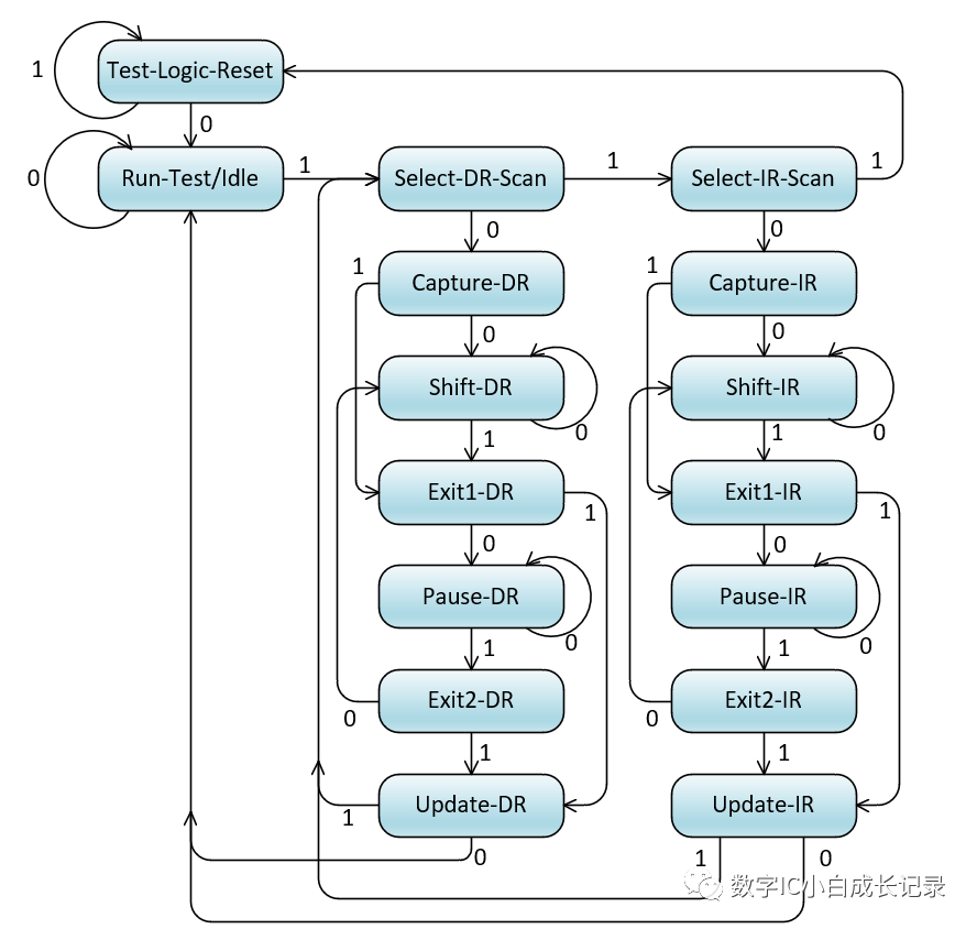
Each state is described as follows:
Test-Logic-Reset: The test logic is disabled, allowing normal system function operations. The instruction register holds either the IDCODE or BYPASS instruction. Furthermore, as can be seen from the above state transition diagram, regardless of the current state of the state machine, after holding ‘1’ on TMS for 5 cycles, it will enter the Test-Logic-Reset state.
Run-Test/Idle: In this state, the instruction in the instruction register is executed, i.e., run-test. For example, if the current instruction is RUNBIST, it will execute the system’s self-test logic. For some instructions that do not trigger execution operations, the state will remain idle.
Select-DR-Scan: A temporary state that decides whether to transition to Capture-DR or Select-IR-Scan based on the next TMS value.
Select-IR-Scan: Also a temporary state that decides whether to transition to Capture-IR or reset to the Test-Logic-Reset state based on the next TMS value.
Exit1-DR/Exit2-DR/Exit1-IR/Exit2-IR: These four are all temporary states that do not perform any operations.
Pause-DR/Pause-IR: In this state, the serial shifting of data (instructions) between TDI and TDO is temporarily halted, keeping its value unchanged. Why is there a pause state? For example, when reading the TDO output through a 32-bit bus, it is necessary to pause after shifting 32 bits to wait for the bus response before continuing to shift data.
Finally, summarizing these 16 states: Although these states seem numerous and complex, it can be observed that, except for the Test-Logic-Reset and Run-Test/Idle states, the remaining states are categorized into operations on DR (data register) and IR (instruction register). Taking IR as an example, it includes 7 states: capture, shift, update, pause, and the two temporary states Exit1 and Exit2. Among these, only the update state will change the output value of the test data or instruction.