
Source: EETOP
Original Author: EETOP Compilation
We need increasingly complex chips and SoCs for all new applications using the latest technologies such as artificial intelligence. For example, Apple’s 5nm SoC A14, which contains 11.8 billion transistors, features a 6-core CPU, a 4-core GPU, and a 16-core NPU engine, capable of performing 11 trillion operations per second; while the AWS 7nm 64-bit Graviton2 custom processor contains even more, at 30 billion transistors. Designing such complex chips requires a standard and verified verification process, which involves extensive verification at various levels using various verification methods and techniques, from IP to subsystems to SoCs.
In this article, let me introduce you to various verification methods used for validating IP, subsystems, and SoCs, and explain why we need new methods/standards like PSS.
For verification engineers handling the SoC verification process, it is crucial to understand how to build electronic systems using SoCs, whether performing white-box verification at the IP level, gray-box verification at the subsystem level, or black-box verification at the SoC level.
How to build electronic systems using SoCs?
Any chip, whether a simple embedded microcontroller or a complex system on a chip [SoC], will have one or more processors. Figure 1 shows a complex electronic system composed of the hardware and software required for electronic devices such as smartphones.
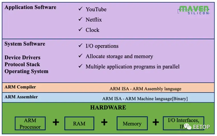
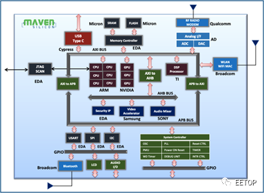
Figure 1: Electronic Systems and SoCs
The hardware consists of a complex SoC that contains almost all the components required by the device. In the case of smartphones, we integrate all hardware components known as IP [Intellectual Property], such as CPUs, GPUs, DSPs, application processors, interface IPs like USB, UART, SPI, I2C, GPIO, as well as system controllers, memory and controllers, Bluetooth, and WiFi, thereby creating the SoC.
The device is composed of application software and system software. Application software provides the user interface, while system software provides the interface that allows application software to interact with hardware. In the case of smartphones, application software can be mobile applications like YouTube, Netflix, Google Maps, while system software can be operating systems [OS] like iOS or Android. System software provides everything from firmware to protocol stacks, as well as the operating system required for the application software to interface with hardware. The operating system manages multiple application threads, memory allocation, and I/O operations in parallel, serving as a core component of system software.
Next, let’s explain how the entire system works, just like a smartphone. For example, when you call an application like the calculator on your smartphone, the operating system loads the executable binary from storage memory into RAM. It then immediately loads its starting address into the program counter [PC] of its processor. The processor [ARM/x86/RISC-V] executes the binary loaded into the RAM/cache pointed to by the PC [RAM address]. This pre-compiled binary is simply the processor’s machine language, so the processor executes the application and computes the result based on its instructions [ADD/SUB/MULT/LOAD].
Understanding the SoC design process using processors can help verification engineers handle any complex subsystem/chip verification at the system level. As part of the SoC verification process, verification engineers may need to deal with various tasks, such as virtual prototyping for system modeling, functional verification of IP, subsystems, and SoCs, hardware-software co-verification, simulation, ASIC prototyping, post-silicon verification, etc. Therefore, it requires a cohesive and complete understanding of both hardware and software to work independently as verification experts, and sometimes close collaboration with software teams is needed to handle software, RTOS/firmware/stack for chip/system-level verification.
Now let’s explore various verification methods.
IP Verification
IP is the fundamental building block of any SoC. Therefore, IP verification requires exhaustive white-box verification, which necessitates methods like formal verification and random simulation, especially for processor IPs, as everything is initiated and driven by them as core components of any SoC. Figure 2 shows how we verify processor IP through exhaustive random simulation based on SystemVerilog UVM TB. All processor instructions can be simulated with various random values, generatingfunctionality, assertions, andcode coverage. We use coverage to measure the progress and quality of verification, followed by final verification sign-off. IP-level verification requires good expertise in HVL programming,formal and dynamic ABV, simulation debugging, and the use of VIP and EDA tools.
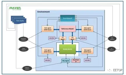
Figure 2 RISC-V UV Verification Environment
ABV – Assertion-Based Verification, VIP – Verification IP
UVM – Universal Verification Method, UVC – UVM Verification Component
The subsystem mainly consists of pre-verified IP and some newly created IP, such as chip-specific bridges and system controllers. Figure 3 shows how we build SoCs from subsystems, where the subsystem integrates all necessary interface IP, bridges, and system controllers using on-chip buses like AMBA. In this case, we prefer simulation-based gray-box verification, especially using random simulation with verification IPs. AllVIP, such as AXI, AHB, APB, GPIO, UART, SPI, and I2C UVC [UVM verification components], will be configured and connected to their respective interfaces. As shown in Figure 3, we create other TB components like reference models, scoreboards, and UVM RAL to enable self-checking of the verification environment. We execute various VIP UVM sequences at the top level, verify data flows, and measure the performance of the bus.
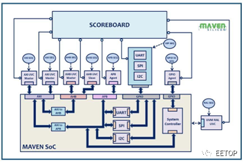
Figure 3 Subsystem UVM Verification Environment
SoC Chip Verification
SoCs are mainly composed of pre-verified third-party IP and some internal IP. Typically, we prefer to use hardware simulation or emulation techniques for black-box verification for SoC-level verification. For example, you may encounter complex SoC verification environments, as shown in Figure 4. The SoC test platform [TB] will have various test platform components such as standard UVM verification IPs [USB/Bluetooth/WiFi and standard interfaces], traditional HDL TB components [JTAG Agent] with UVM wrappers, custom UVM agents [firmware agents], as well as some displays, scoreboards, and SystemC/C/C++ functional models. In this case, you will have to handle firmware and UVM sequences at the chip level. As a verification engineer, you need to know how to implement such a mixed verification environment using standard VIP, traditional HDL BVM, and firmware code, and more importantly, understand how to automate simulation/emulation using EDA tools.
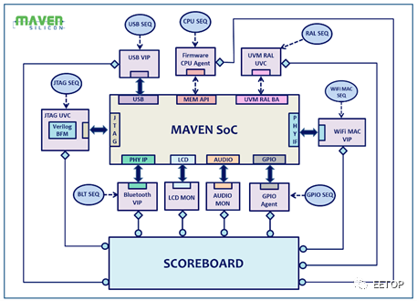
Figure 4: SoC Verification Environment
UVM – Universal Verification Method, UVC – UVM Verification Component
BFM Bus Functional Model, VIP Verification IP, RAL Register Abstraction Layer
Let me explain how it works. For example, if the SoC uses an ARM processor, we usually replace the ARM RTL [encrypted netlist/RTL] with its functional model called DSM [Design Simulation Model], which can use firmware [written in C] as stimulus to initiate any operation and drive all other peripherals [RTL IP]. Therefore, SoC verifiers write UVM sequences, generating various directed scenarios through firmware test cases, and verifying SoC functionality. During simulation, the firmware C source code is compiled into target code [ARM machine language binary], which will be loaded into on-chip RAM. The ARM processor model [DSM] reads the target code from memory and initiates operations by configuring and driving all RTL peripheral modules [Verilog/VHDL]. It is applicable for simulation and emulation. If the SoC is very complex, hardware emulation is preferred to speed up the verification process and achieve faster verification sign-off.
Why Choose PSS?
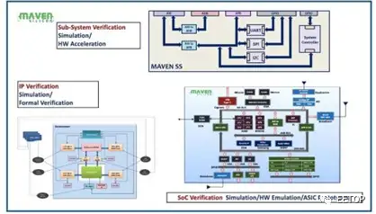
Figure 5: IP, Subsystem, and SoC Verification Methods
PSS Definition: The Portable Stimulus Standard defines a specification for creating a single representation of stimuli and test scenarios that can be used by various users at different integration levels under different configurations, thereby enabling the generation of different implementations of scenarios that run on various execution platforms, including but not limited to simulation, emulation, FPGA prototyping, and post-silicon. Using this standard, users can specify a set of behaviors once, from which multiple implementations can be derived.
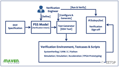
Figure 6: PSS Process
As shown in Figure 6, using PSS, we can define test scenarios and execute them using any verification technique at any level of IP/subsystem/SoC. For example, we can define test scenarios for IP in PSS. In IP-level verification, we can use EDA tools to generate assertions from its PSS specifications for formal verification, and if needed, we can generate UVM test cases from the same PSS specification for SoC-level simulation or emulation. We do not need to manually rewrite IP/subsystem-level test cases to migrate and reuse them at the SoC level. The PSS specification remains unchanged for various technologies. Depending on our choice, such as formal/simulation/emulation, EDA tools can generate test cases from any language or method (such as C/C++/Verilog/SystemVerilog/UVM) in PSS form.
Formal verification and methods like PSS are continuously evolving, while EDA vendors are also using technologies like ML to automatically generate tests and verification sign-off. Therefore, in the near future, the industry will need talented and technically skilled verification engineers who can collaborate with chip architects to drive the verification process for first silicon success through a “design for verification” approach, rather than just traditional verification personnel dealing with black-box verification primarily involved in writing test cases and managing regression tests. Are you interested in chip verification and ready for this important work?
Editor: Lu Dingci