EETOP focuses on chips and microelectronics, click the blue text above to follow us.
Source:wikichip
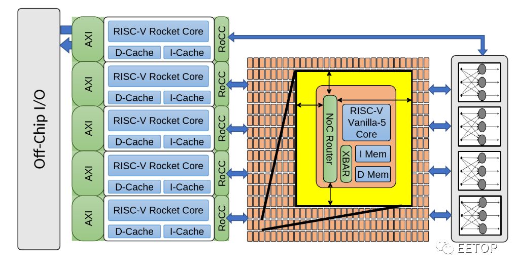
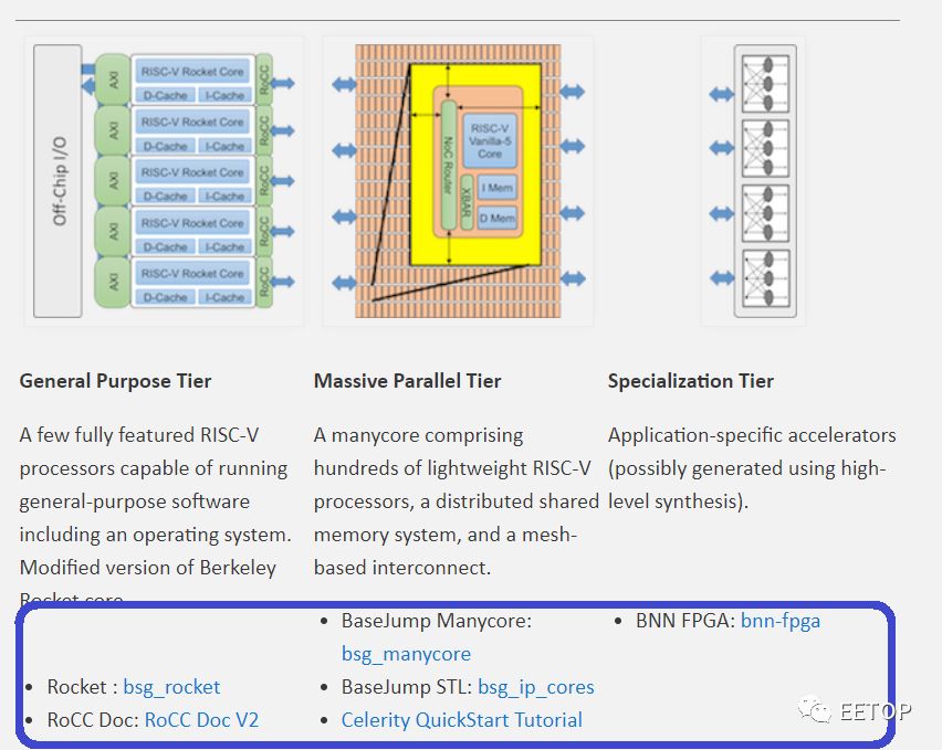
Next, let’s provide a quick overview of the entire Celerity SoC. Celerity is a multi-core, multi-layer AI accelerator. Overall, the chip includes three main layers: a general-purpose layer, a massively parallel layer, and a specialized layer. Why use a layered SoC? The main reason is to achieve high flexibility and greater power efficiency in typical CPU designs (although the efficiency is not as high as that of ASIC NPUs). The general-purpose layer can perform almost any operation: general computation, memory management, and control of the rest of the chip. Therefore, they integrated five high-performance out-of-order RISC-V Rocket cores from the Free Chip Project. The next layer is the massively parallel layer, which integrates 496 low-power custom-designed RISC-V cores into a grid. These custom cores, called Vanilla-5, are in-order scalar cores that take up 40 times less space than Rocket cores. The final layer is the specialized layer that integrates a binary neural network (BNN) accelerator. These three layers are tightly linked and interface with DDR memory at 400 MHz.
The manycore mesh clock on Celerity is provided by a custom PLL. This is a fairly simple first-order ΔΣ frequency digital converter (FDC) PLL. The implementation unit consists of 16 DCOs forming a group, each implementation unit being a ring oscillator, where the inverting elements load the NAND gate circuit as shown in the slide below. This is done to implement the entire design using only standard cells. To this end, the entire digital PLL is a fully synthesizable and automatically placed and routed design. The PLL operates at a frequency range of 10 MHz to 3.3GHz on its 16-nanometer chip.

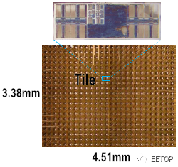
As with many academic projects, silicon area is also very important; the entire chip measures 25 square millimeters (5×5). For Celerity, many key architectural design decisions were driven by the need to limit silicon area, which means reduced complexity. The manycore itself is a 16 by 31 array of Vanilla-5 RISC-V small cores. The 32nd row of this array is used for an external host that connects to other components on the chip (e.g., sending messages/data to the Rocket cores for final processing). The entire grid measures 3.38 mm by 4.51 mm (15.24 mm²), accounting for about 61% of the entire chip. Vanilla-5 cores are 5-stage in-order pipelined RV32IM cores, thus supporting integer and multiplication extensions. In silicon chip implementations, these cores can achieve 1.4 GHz, which is 350 MHz higher than the first silicon chip they showcased at Hot Chips 29.
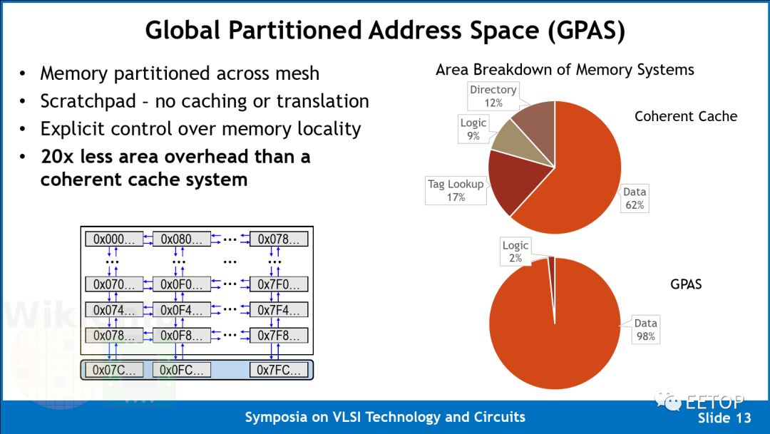
To reduce the complexity of the manycore array, Celerity utilizes a partitioned global address space for on-chip packet and remote storage programming models.
The array takes advantage of a Global Partitioned Address Space (GPAS). In other words, instead of using caches, a 32-bit addressing scheme maps the entire memory address space to all nodes in the network. This approach also means no virtualization or translation is needed, greatly simplifying the design. They claim that this design can reduce regional overhead by 20 times compared to an equivalent coherent cache system. It is worth noting that since the target workload of this manycore array is AI acceleration (as opposed to more general computing), they can adopt an explicitly partitioned register storage scheme, as these workloads exhibit highly parallel, well-defined independent stream patterns. Furthermore, for this type of code, the ability to control memory locality can prove to be very beneficial. Each core in the array can freely execute loads and stores to any local address; however, it can only execute stores to remote addresses. No remote loads mean they reduced router area by 10%, and since remote storage can be pipelined, it can prevent pipeline stalls.
This remote storage programming model allows them to use two networks, one data network and a credit network for managing outstanding storage.
As mentioned earlier, the 32nd row is used for an external host. In practice, this means memory mapping extends to 16 routing docking points located at the bottom of the array, allowing messages to enter and exit the manycore array, reaching the large cores and other peripherals on the chip.
Celerity does not use the very common wormhole routing (used by Kilocore, Piton, Tile64, etc.), but instead combines address and data into a single flit packet. This design eliminates the header/footer information needed for sending both data and metadata. Additionally, since there is no reserved routing, it eliminates HOL blocking. Each flit is 80 bits wide – control bits 16 bits, data bits 32 bits, node address bits 10 bits, memory address bits 22 bits. Flit node addresses retain the ability to send data to any destination. The main benefit of this design is that by injecting only a single flit into the network, a single ordered pipeline can execute a store every cycle.
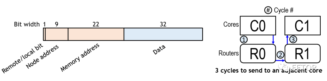
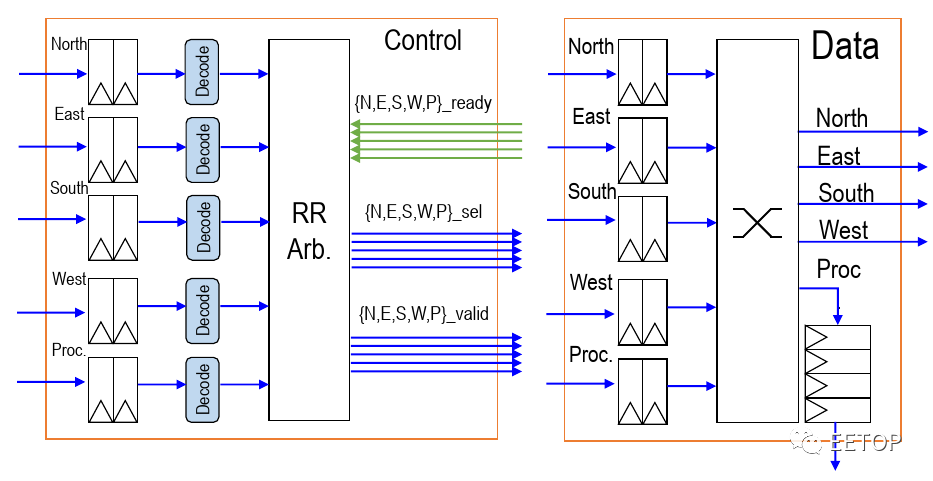
In the manycore array of 496 nodes, each node has a router. The router itself contains two FIFO elements at the input of each basic direction (N, S, E, W), and a control processor that serves as temporary storage in case of network congestion. They use round-robin arbitration to determine the priority of packets, allowing arbitration for each direction in each cycle. They use size-ordered routing (reducing offset in one direction before moving to another direction). With a simple design, they can implement the entire routing as a single-stage design, with no pipeline registers between nodes. In other words, each hop requires only one cycle. For example, the delay for any adjacent core storage area is only 3 cycles – turning to local routing, jumping to adjacent routing, and finally going to the neighbor’s memory space, with the router and core located in the same clock domain, meaning they can also operate at frequencies of up to 1.4 GHz.
There are two networks – one data network and one credit counter network. The router uses a source-controlled credit counter that decrements every time a remote storage packet is injected into the network. The credit counter network returns using the same architecture as the data described above, but only 9 bits, as it only contains node addresses.
So, what does this mean? The Celerity team reported operating frequencies from 500 MHz to 1.4 GHz at 600 mV to 980 mV. We believe Celerity is now the second highest clock frequency university chip, second only to Kilocore (although it is worth noting that due to packaging limitations, Kilocore can only support 160 of its 1000 cores). At 1.4 GHz, the entire grid’s maximum computational capability is 694.4 INT 32 GOPS. They report their numbers in Giga-RISC-V instructions per second (GRVIS) rather than GOPS to emphasize the fact that these instructions are complete RISC-V instructions, not just integer operations. Note that since the Vanilla-5 cores are RV32IM, they support RISC-V integer and multiplication extensions but do not support floating-point operations, meaning all AI workloads must be quantized. Because the routers that interconnect the nodes are in the same clock domain as the cores, each router supports 5 flits per cycle, giving each node a total aggregate bandwidth of 748 Gbps, with a total aggregate network bandwidth of 371 Tb/s.
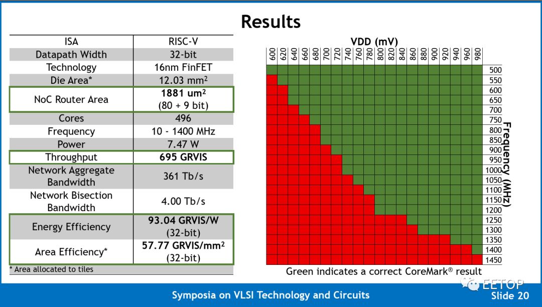
Unfortunately, the Celerity team did not report any common AI-related benchmark results. Instead, they chose to use CoreMark, achieving a total score of 812350 at 580.25 CoreMark/MHz. CoreMark has been a benchmark for the RISC-V community over the past few years. The issue with CoreMark is that it often generates incredibly optimistic scores for simple in-order designs that seem to compete well with tuned modern out-of-order designs, while real-world workloads show very different results. Given that the premise of this chip is to produce a highly flexible AI accelerator, we hope to encourage the Celerity team to produce more meaningful results, such as formal MLPerf submissions.
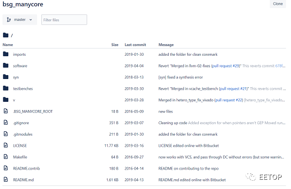
Celerity’s open-source RTL design has been publicly released on the Celerity website (Open Source Link:http://opencelerity.org/), with partial screenshots as shown below:
Click to read the original article for open-source information.