Disassembly Event in Breadboard Community,Drone, Handheld Oscilloscope、Computer、Robot Vacuum、Smartwatch、Solid State Drive、Portable Speaker,Great Prizes and Lots of Benefits, Welcome to Join!More Details👈 Author: Little Devil owo, Source: Breadboard Community [Write Disassembly, Win Drone Activity]Introduction
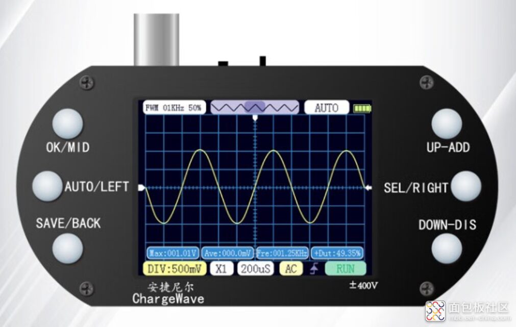
When I was studying analog electronics, I thought I should buy an oscilloscope to observe experimental phenomena, but I struggled with a lack of funds, so I bought a mini oscilloscope online. The data sampling rate is 2.5MHz, and the bandwidth is 500KHz. This data can only show the general waveform, let alone any details. What do you all think? I believe this mini oscilloscope can only show waveform changes, but it is very difficult to use for projects. Today, I will disassemble it and share with you to see its workmanship and the chips used, to see if it is worth the price of a hundred yuan.
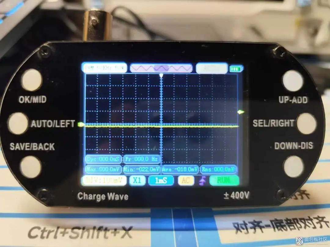
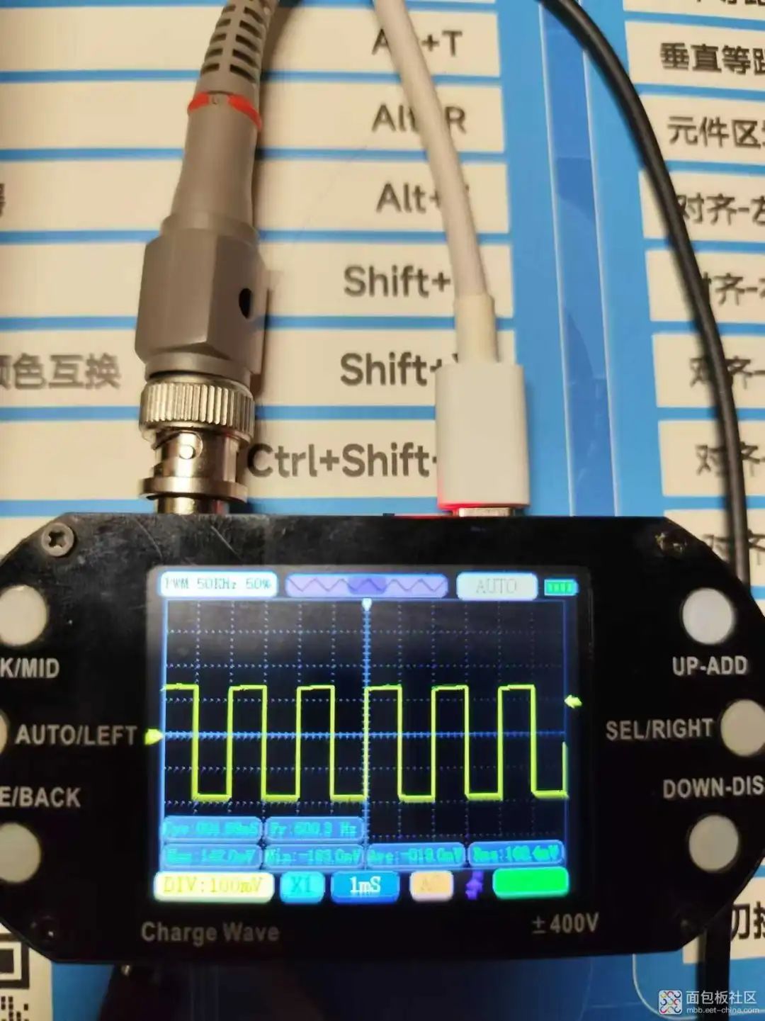
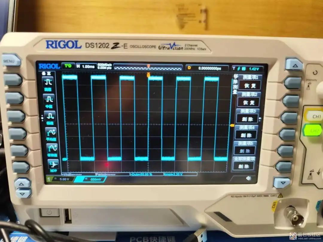
Waveform Test (50Hz Square Wave)For this most basic waveform, the mini oscilloscope can start to display it, and it is not much different from what a normal oscilloscope measures.
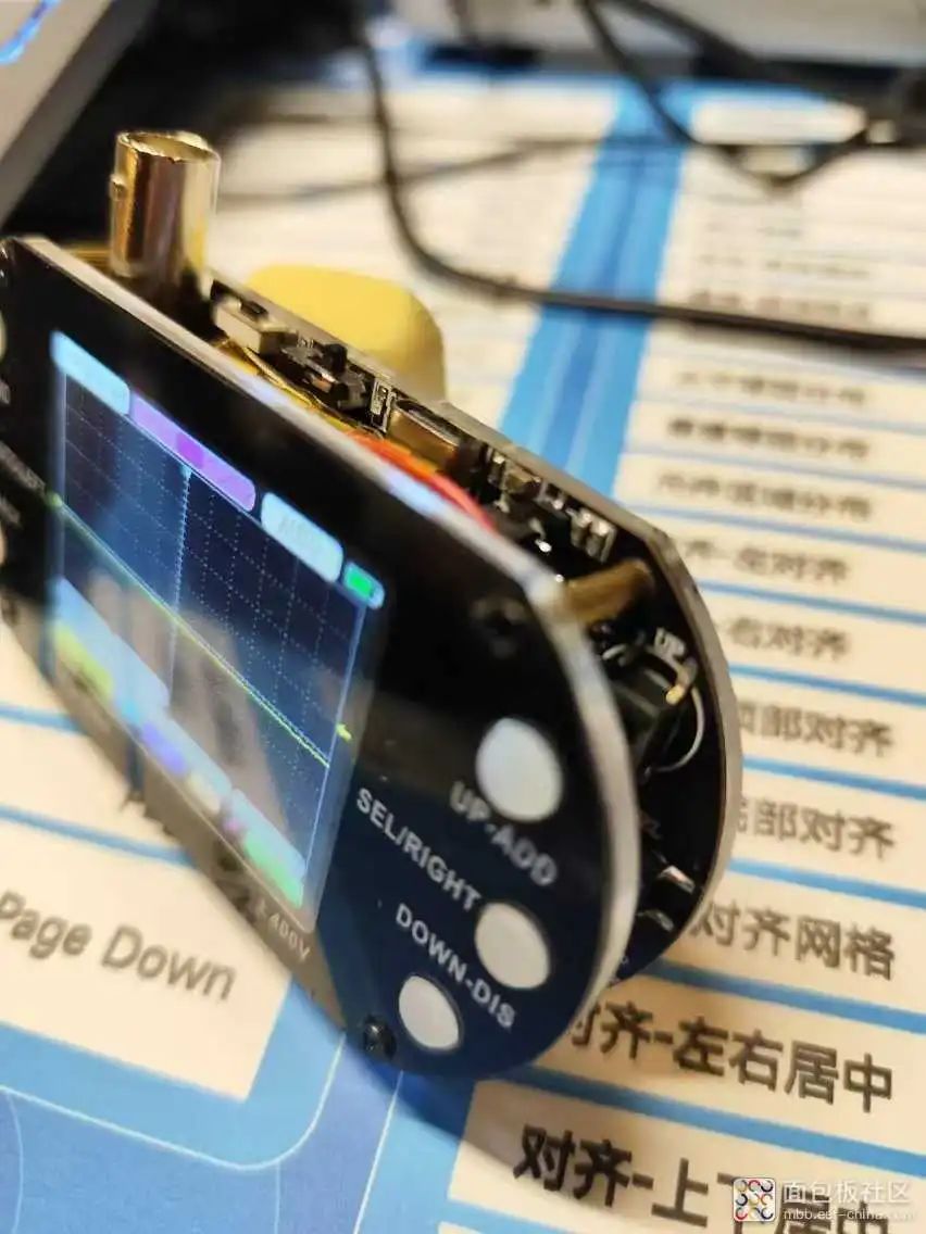
Disassembly Process(1) First, unscrew the four screws on the back cover, take off the back cover and the acrylic plate.
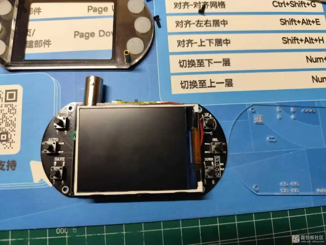
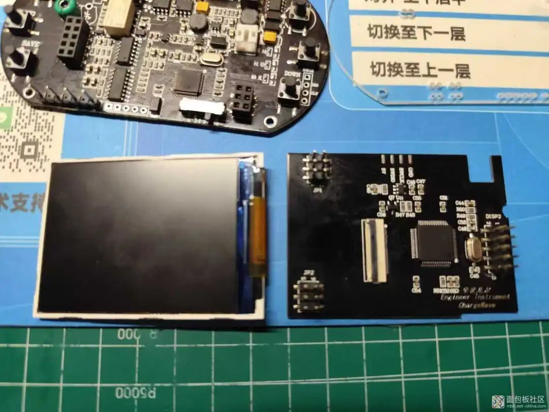
(2) Then you can see the screen module and buttons, be careful not to lose the button caps on the buttons.
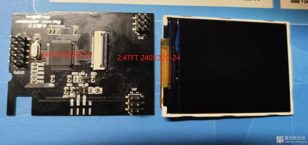
(3) The screen module can be disassembled separately via 3 sets of pin headers.
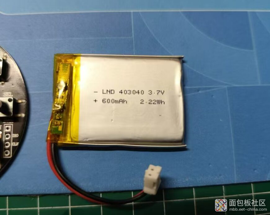
(4) The battery is connected to the mainboard via a ribbon cable and can be removed. This should be convenient for later replacement.
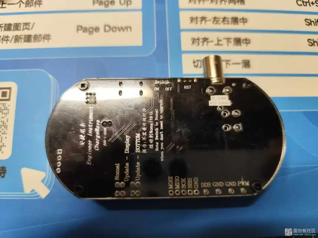
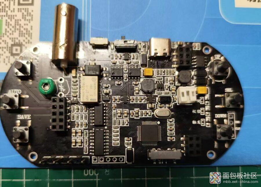
(5) The mainboard looks quite clean and clear, and the layout is also good.
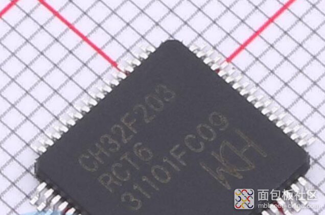
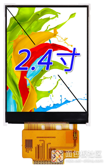
Screen ModuleThe main control of the screen uses a CH32F203RCT6 chip, and the screen is a 2.4-inch TFT screen with 24 pins; the screen driver should be ST7789. Data sheet: https://item.szlcsc.com/5744905.html
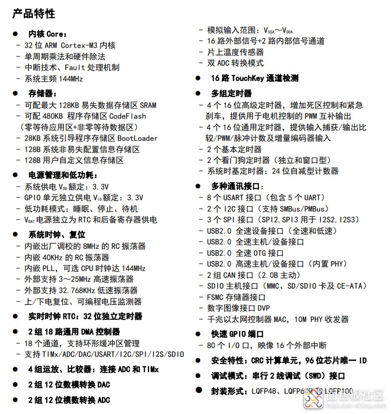
The Cortex-M3 core designed is an industrial-grade general-purpose microcontroller. The series products have a main frequency of up to 144MHz, and the GPIO voltage is isolated (separated from system power supply). Resources have increased to include a random number unit, 4 operational amplifier comparators, touch detection, and increased the number of USART/UART ports to 8, and motor timers to 4. Among the dedicated interfaces: USB2.0 high-speed interface (480Mbps) has a built-in PHY transceiver, Ethernet MAC reaches gigabit, and integrates a 10M-PHY module, etc. Coupled with clock safety, power management, dual DMA, ADC, DAC, SPI, I2C, DVP, SDIO, CAN, FSMC and other resources, it can be applied to multi-acquisition and multi-communication scenarios.
Author: Little Devil owo, Source: Breadboard Community [Write Disassembly, Win Drone Activity]Introduction
When I was studying analog electronics, I thought I should buy an oscilloscope to observe experimental phenomena, but I struggled with a lack of funds, so I bought a mini oscilloscope online. The data sampling rate is 2.5MHz, and the bandwidth is 500KHz. This data can only show the general waveform, let alone any details. What do you all think? I believe this mini oscilloscope can only show waveform changes, but it is very difficult to use for projects. Today, I will disassemble it and share with you to see its workmanship and the chips used, to see if it is worth the price of a hundred yuan.
Waveform Test (50Hz Square Wave)For this most basic waveform, the mini oscilloscope can start to display it, and it is not much different from what a normal oscilloscope measures.
Disassembly Process(1) First, unscrew the four screws on the back cover, take off the back cover and the acrylic plate.
(2) Then you can see the screen module and buttons, be careful not to lose the button caps on the buttons.
(3) The screen module can be disassembled separately via 3 sets of pin headers.
(4) The battery is connected to the mainboard via a ribbon cable and can be removed. This should be convenient for later replacement.
(5) The mainboard looks quite clean and clear, and the layout is also good.
Screen ModuleThe main control of the screen uses a CH32F203RCT6 chip, and the screen is a 2.4-inch TFT screen with 24 pins; the screen driver should be ST7789. Data sheet: https://item.szlcsc.com/5744905.html
The Cortex-M3 core designed is an industrial-grade general-purpose microcontroller. The series products have a main frequency of up to 144MHz, and the GPIO voltage is isolated (separated from system power supply). Resources have increased to include a random number unit, 4 operational amplifier comparators, touch detection, and increased the number of USART/UART ports to 8, and motor timers to 4. Among the dedicated interfaces: USB2.0 high-speed interface (480Mbps) has a built-in PHY transceiver, Ethernet MAC reaches gigabit, and integrates a 10M-PHY module, etc. Coupled with clock safety, power management, dual DMA, ADC, DAC, SPI, I2C, DVP, SDIO, CAN, FSMC and other resources, it can be applied to multi-acquisition and multi-communication scenarios.
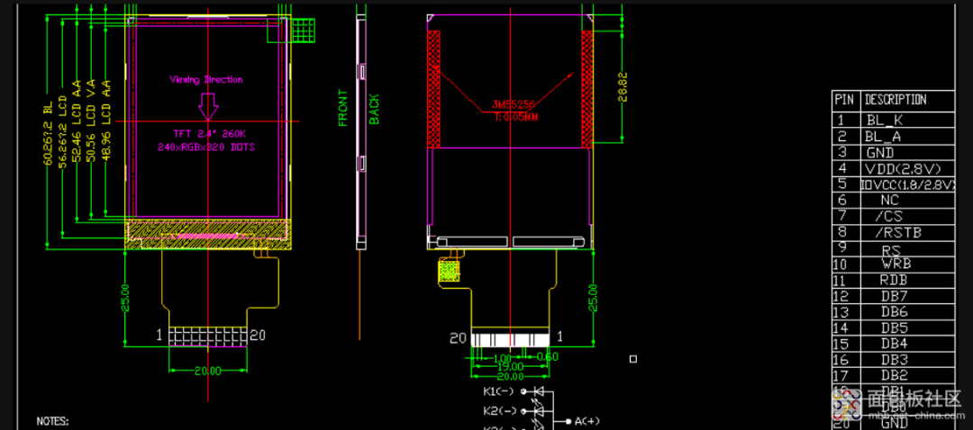 Most of the 2.4 TFT screens online are 10 pins; I have not found data for 24 pins, but found a 20-pin version, which should be compatible. For the CH32F203RCT6 chip, driving this screen is more than enough, but there is less information available online, so I will share similar LCD code with you. I must say that the LCD design of this product is really beautiful, and it seems that a lot of effort was spent researching the UI.
#include "lcd.h"
#include "stdlib.h"
#include "font.h"
#include "stdarg.h"
#define  LCD_CMD         ((u32)0x6001FFFF)
#define  LCD_DATA        ((u32)0x60020000)

#define LCD_CLEAR_SEND_NUMBER 5760
u16 BACK_COLOR = BLACK, FORE_COLOR = WHITE;
void lcd_write_cmd(const u8 cmd){    *(__IO u8*)LCD_CMD=cmd;}
void lcd_write_data(const u8 data){    *(__IO u8*)LCD_DATA=data;}
void lcd_write_half_word(const u16 da){    *(__IO u8*)LCD_DATA=(u8)(da>>8);    *(__IO u8*)LCD_DATA=(u8)da;}
u8 lcd_read_data(void){    vu8 ram;    ram = *(__IO u8*)LCD_DATA;    return ram;}
u8 lcd_read_reg(const u8 reg){    lcd_write_cmd(reg);    delay_us(5);    return lcd_read_data();}
void lcd_fsmc_init(void){    GPIO_InitTypeDef GPIO_InitStructure={0};    FSMC_NORSRAMInitTypeDef  FSMC_NORSRAMInitStructure={0};    FSMC_NORSRAMTimingInitTypeDef  readWriteTiming={0};    FSMC_NORSRAMTimingInitTypeDef  writeTiming={0};
    RCC_AHBPeriphClockCmd(RCC_AHBPeriph_FSMC,ENABLE);    RCC_APB2PeriphClockCmd(RCC_APB2Periph_GPIOB|RCC_APB2Periph_GPIOD|RCC_APB2Periph_GPIOE|RCC_APB2Periph_GPIOG,ENABLE);
    GPIO_InitStructure.GPIO_Pin = GPIO_Pin_14;    GPIO_InitStructure.GPIO_Mode = GPIO_Mode_Out_PP;    GPIO_InitStructure.GPIO_Speed = GPIO_Speed_50MHz;    GPIO_Init(GPIOB, &GPIO_InitStructure);
    GPIO_InitStructure.GPIO_Pin = GPIO_Pin_0|GPIO_Pin_1|GPIO_Pin_4|GPIO_Pin_5|GPIO_Pin_8|GPIO_Pin_9|GPIO_Pin_10|GPIO_Pin_14|GPIO_Pin_15;    GPIO_InitStructure.GPIO_Mode = GPIO_Mode_AF_PP;    GPIO_InitStructure.GPIO_Speed = GPIO_Speed_50MHz;    GPIO_Init(GPIOD, &GPIO_InitStructure);
    GPIO_InitStructure.GPIO_Pin = GPIO_Pin_7|GPIO_Pin_8|GPIO_Pin_9|GPIO_Pin_10|GPIO_Pin_11|GPIO_Pin_12|GPIO_Pin_13|GPIO_Pin_14|GPIO_Pin_15;    GPIO_InitStructure.GPIO_Mode = GPIO_Mode_AF_PP;    GPIO_InitStructure.GPIO_Speed = GPIO_Speed_50MHz;    GPIO_Init(GPIOE, &GPIO_InitStructure);
    /*   RS--D12  */    GPIO_InitStructure.GPIO_Pin = GPIO_Pin_12;    GPIO_InitStructure.GPIO_Mode = GPIO_Mode_AF_PP;    GPIO_InitStructure.GPIO_Speed = GPIO_Speed_50MHz;    GPIO_Init(GPIOD, &GPIO_InitStructure);
    /* CS: PD11*/    GPIO_InitStructure.GPIO_Pin = GPIO_Pin_11;    GPIO_InitStructure.GPIO_Mode = GPIO_Mode_Out_PP;    GPIO_InitStructure.GPIO_Speed = GPIO_Speed_50MHz;    GPIO_Init(GPIOD, &GPIO_InitStructure);    GPIO_ResetBits(GPIOD,GPIO_Pin_11);
    readWriteTiming.FSMC_AddressSetupTime = 0x01;    readWriteTiming.FSMC_AddressHoldTime = 0x00;    readWriteTiming.FSMC_DataSetupTime = 0x0f;    readWriteTiming.FSMC_BusTurnAroundDuration = 0x00;    readWriteTiming.FSMC_CLKDivision = 0x00;    readWriteTiming.FSMC_DataLatency = 0x00;    readWriteTiming.FSMC_AccessMode = FSMC_AccessMode_A;
    writeTiming.FSMC_AddressSetupTime = 0x00;    writeTiming.FSMC_AddressHoldTime = 0x00;    writeTiming.FSMC_DataSetupTime = 0x03;    writeTiming.FSMC_BusTurnAroundDuration = 0x00;    writeTiming.FSMC_CLKDivision = 0x00;    writeTiming.FSMC_DataLatency = 0x00;    writeTiming.FSMC_AccessMode = FSMC_AccessMode_A;
    FSMC_NORSRAMInitStructure.FSMC_Bank = FSMC_Bank1_NORSRAM1;
    FSMC_NORSRAMInitStructure.FSMC_DataAddressMux = FSMC_DataAddressMux_Disable;    FSMC_NORSRAMInitStructure.FSMC_MemoryType =FSMC_MemoryType_SRAM;    FSMC_NORSRAMInitStructure.FSMC_MemoryDataWidth = FSMC_MemoryDataWidth_8b;    FSMC_NORSRAMInitStructure.FSMC_BurstAccessMode =FSMC_BurstAccessMode_Disable;    FSMC_NORSRAMInitStructure.FSMC_WaitSignalPolarity = FSMC_WaitSignalPolarity_Low;    FSMC_NORSRAMInitStructure.FSMC_AsynchronousWait=FSMC_AsynchronousWait_Disable;    FSMC_NORSRAMInitStructure.FSMC_WrapMode = FSMC_WrapMode_Disable;    FSMC_NORSRAMInitStructure.FSMC_WaitSignalActive = FSMC_WaitSignalActive_BeforeWaitState;    FSMC_NORSRAMInitStructure.FSMC_WriteOperation = FSMC_WriteOperation_Enable;    FSMC_NORSRAMInitStructure.FSMC_WaitSignal = FSMC_WaitSignal_Disable;    FSMC_NORSRAMInitStructure.FSMC_ExtendedMode = FSMC_ExtendedMode_Enable;    FSMC_NORSRAMInitStructure.FSMC_WriteBurst = FSMC_WriteBurst_Disable;    FSMC_NORSRAMInitStructure.FSMC_ReadWriteTimingStruct = &readWriteTiming    FSMC_NORSRAMInitStructure.FSMC_WriteTimingStruct = &writeTiming    FSMC_NORSRAMInit(&FSMC_NORSRAMInitStructure);    FSMC_NORSRAMCmd(FSMC_Bank1_NORSRAM1, ENABLE);
}
/******************************************************************************** Function Name  : TIM1_PWMOut_Init* Description    : Initializes TIM1 PWM output.* Input          : arr: the period value.*                  psc: the prescaler value.*                                    ccp: the pulse value.* Return         : None*******************************************************************************/void TIM1_PWMOut_Init( u16 arr, u16 psc, u16 ccp ){    GPIO_InitTypeDef GPIO_InitStructure;    TIM_OCInitTypeDef TIM_OCInitStructure;    TIM_TimeBaseInitTypeDef TIM_TimeBaseInitStructure;
    RCC_APB2PeriphClockCmd( RCC_APB2Periph_GPIOB | RCC_APB2Periph_TIM1, ENABLE );    GPIO_InitStructure.GPIO_Pin = GPIO_Pin_14;    GPIO_InitStructure.GPIO_Mode = GPIO_Mode_AF_PP;    GPIO_InitStructure.GPIO_Speed = GPIO_Speed_50MHz;    GPIO_Init( GPIOB, &GPIO_InitStructure );    TIM_TimeBaseInitStructure.TIM_Period = arr;    TIM_TimeBaseInitStructure.TIM_Prescaler = psc;    TIM_TimeBaseInitStructure.TIM_ClockDivision = TIM_CKD_DIV1;    TIM_TimeBaseInitStructure.TIM_CounterMode = TIM_CounterMode_Up;    TIM_TimeBaseInit( TIM1, &TIM_TimeBaseInitStructure);
#if (PWM_MODE == PWM_MODE1)  TIM_OCInitStructure.TIM_OCMode = TIM_OCMode_PWM1;
#elif (PWM_MODE == PWM_MODE2)    TIM_OCInitStructure.TIM_OCMode = TIM_OCMode_PWM2;
#endif
    TIM_OCInitStructure.TIM_OutputState = TIM_OutputState_Enable;    TIM_OCInitStructure.TIM_Pulse = ccp;    TIM_OCInitStructure.TIM_OCPolarity = TIM_OCPolarity_High;    TIM_OC1Init( TIM1, &TIM_OCInitStructure );    TIM_CtrlPWMOutputs(TIM1, ENABLE );    TIM_OC1PreloadConfig( TIM1, TIM_OCPreload_Disable );    TIM_ARRPreloadConfig( TIM1, ENABLE );    TIM_Cmd( TIM1, ENABLE );}
void lcd_gpio_init(void){    GPIO_InitTypeDef  GPIO_InitStructure;
    RCC_APB2PeriphClockCmd(RCC_APB2Periph_GPIOD, ENABLE);
    GPIO_InitStructure.GPIO_Pin = GPIO_Pin_13;    GPIO_InitStructure.GPIO_Mode = GPIO_Mode_Out_PP;    GPIO_InitStructure.GPIO_Speed = GPIO_Speed_50MHz;    GPIO_Init(GPIOD, &GPIO_InitStructure);    GPIO_SetBits(GPIOD,GPIO_Pin_13);
    GPIO_ResetBits(GPIOD,GPIO_Pin_13);    //wait at least 100ms for reset    delay_ms(100);    GPIO_SetBits(GPIOD,GPIO_Pin_13);//    TIM1_PWMOut_Init( 1000, 48000-1, 50 );}
void lcd_init(void){    u16 id=0;    lcd_gpio_init();    lcd_fsmc_init();
    lcd_write_cmd(0X04);    id = lcd_read_data();      //dummy read    id = lcd_read_data();      //read 0X85    id = lcd_read_data();      //read 0X85    id <<= 8;    id |= lcd_read_data();     //read 0X52
    printf("id = %x\r\n",id);    delay_ms(50);
    /* Memory Data Access Control */    lcd_write_cmd(0x36);    lcd_write_data(0x00);    /* RGB 5-6-5-bit  */    lcd_write_cmd(0x3A);    lcd_write_data(0x05);    /* Porch Setting */    lcd_write_cmd(0xB2);    lcd_write_data(0x0C);    lcd_write_data(0x0C);    lcd_write_data(0x00);    lcd_write_data(0x33);    lcd_write_data(0x33);    /*  Gate Control */    lcd_write_cmd(0xB7);    lcd_write_data(0x00);    /* VCOM Setting */    lcd_write_cmd(0xBB);    lcd_write_data(0x3F);    /* LCM Control */    lcd_write_cmd(0xC0);    lcd_write_data(0x2C);    /* VDV and VRH Command Enable */    lcd_write_cmd(0xC2);    lcd_write_data(0x01);    /* VRH Set */    lcd_write_cmd(0xC3);    lcd_write_data(0x0D);    /* VDV Set */    lcd_write_cmd(0xC4);    lcd_write_data(0x20);
    /* Frame Rate Control in Normal Mode */    lcd_write_cmd(0xC6);    lcd_write_data(0x03);    //60Hz-0x0F   82Hz-0x07  99Hz-0x03
    /* Power Control 1 */    lcd_write_cmd(0xD0);    lcd_write_data(0xA4);    lcd_write_data(0xA1);    /* Positive Voltage Gamma Control */    lcd_write_cmd(0xE0);    lcd_write_data(0xF0);    lcd_write_data(0x03);    lcd_write_data(0x09);    lcd_write_data(0x03);    lcd_write_data(0x03);    lcd_write_data(0x10);    lcd_write_data(0x2D);    lcd_write_data(0x43);    lcd_write_data(0x3F);    lcd_write_data(0x33);    lcd_write_data(0x0D);    lcd_write_data(0x0E);    lcd_write_data(0x29);    lcd_write_data(0x32);    /* Negative Voltage Gamma Control */    lcd_write_cmd(0xE1);    lcd_write_data(0xF0);    lcd_write_data(0x0C);    lcd_write_data(0x10);    lcd_write_data(0x0E);    lcd_write_data(0x0E);    lcd_write_data(0x0A);    lcd_write_data(0x2D);    lcd_write_data(0x33);    lcd_write_data(0x45);    lcd_write_data(0x3A);    lcd_write_data(0x14);    lcd_write_data(0x19);    lcd_write_data(0x31);    lcd_write_data(0x37);    /* Display Inversion On */    lcd_write_cmd(0x21);    /* Sleep Out */    lcd_write_cmd(0x11);    /* wait for power stability */    delay_ms(100);
    lcd_clear(BLACK);
    /* display on */    GPIO_SetBits(GPIOB,GPIO_Pin_14);    lcd_write_cmd(0x29);
}
/** * Set background color and foreground color * * @param   back    background color * @param   fore    fore color * * @return  void */void lcd_set_color(u16 back, u16 fore){    BACK_COLOR = back;    FORE_COLOR = fore;}
void lcd_display_on(void){    GPIO_SetBits(GPIOB,GPIO_Pin_14);}
void lcd_display_off(void){    GPIO_ResetBits(GPIOB,GPIO_Pin_14);}
/* lcd enter the minimum power consumption mode and backlight off. */void lcd_enter_sleep(void){    GPIO_ResetBits(GPIOB,GPIO_Pin_14);    delay_ms(5);    lcd_write_cmd(0x10);}
/* lcd turn off sleep mode and backlight on. */void lcd_exit_sleep(void){    GPIO_SetBits(GPIOB,GPIO_Pin_14);    delay_ms(5);    lcd_write_cmd(0x11);    delay_ms(120);}
/** * Set drawing area * * @param   x1      start of x position * @param   y1      start of y position * @param   x2      end of x position * @param   y2      end of y position * * @return  void */void lcd_address_set(u16 x1, u16 y1, u16 x2, u16 y2){    lcd_write_cmd(0x2a);    lcd_write_data(x1 >> 8);    lcd_write_data(x1);    lcd_write_data(x2 >> 8);    lcd_write_data(x2);
    lcd_write_cmd(0x2b);    lcd_write_data(y1 >> 8);    lcd_write_data(y1);    lcd_write_data(y2 >> 8);    lcd_write_data(y2);
    lcd_write_cmd(0x2C);}
/** * clear the lcd. * * @param   color       Fill color * * @return  void */void lcd_clear(u16 color){    u16 i, j;    u8 data[2] = {0};
    data[0] = color >> 8;    data[1] = color;    lcd_address_set(0, 0, LCD_W - 1, LCD_H - 1);
    /* 5760 = 240*240/20 */
        for (i = 0; i < LCD_W; i++)        {            for (j = 0; j < LCD_H; j++)            {                *(__IO u8*)LCD_DATA=data[0];                *(__IO u8*)LCD_DATA=data[1];            }        }
}
/** * display a point on the lcd. * * @param   x   x position * @param   y   y position * * @return  void */
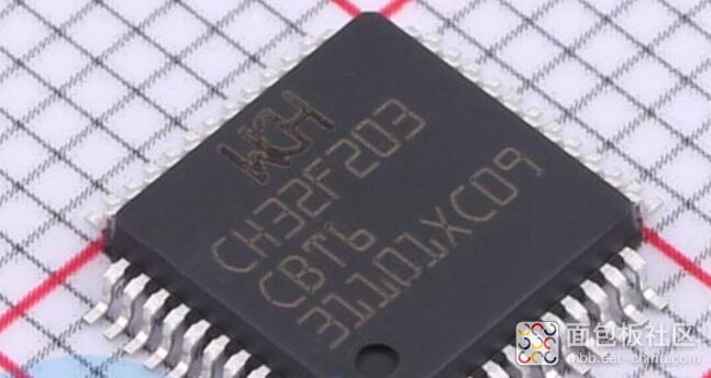
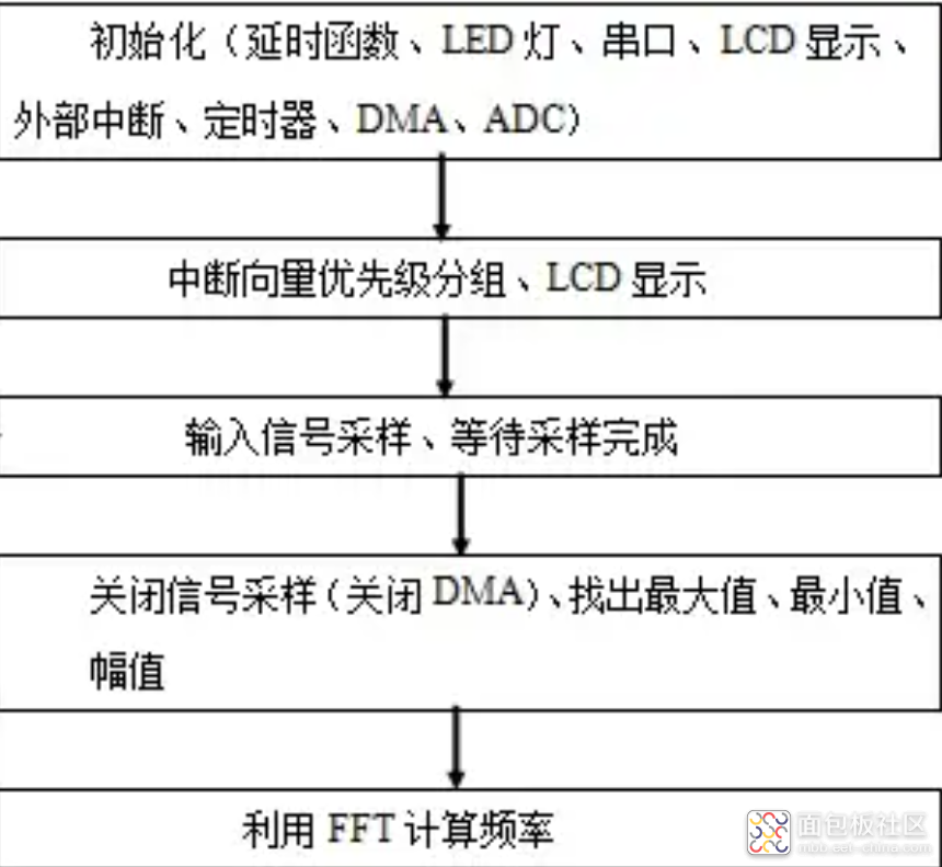 The principle of the oscilloscope can be simply explained, but I am not clear about the method used in this product, so I will provide an idea.1. Signal Input and Preprocessing1. Signal Input: The measured voltage signal first enters the acquisition front end of the digital oscilloscope.2. Preprocessing: At the acquisition front end, the signal will be processed through components such as preamplifiers and filters. The preamplifier is used to adjust the signal amplitude to meet the needs of subsequent processing; the filter is used to filter out unwanted frequency components to improve the signal-to-noise ratio.2. Analog to Digital Conversion (A/D Conversion)1. Analog-to-Digital Converter (ADC): The preprocessed analog signal is sent to the ADC. The ADC’s function is to convert the analog signal into a digital signal. This conversion process includes sampling and quantization, that is, discretizing the continuous analog signal in time and quantizing it into a series of digital values in amplitude.2. Digital Signal Storage: The converted digital signal is stored in the internal memory of the digital oscilloscope, such as FLASH or DDRAM, etc. These memories have high speed and large capacity, capable of real-time saving a large amount of sampled data.3. Data Processing and Display1. Data Processing: The digital signal stored in the internal memory can undergo various analyses and processing through software programming, such as waveform reconstruction, spectrum analysis, noise suppression, etc. These processing functions enable the digital oscilloscope to provide richer and more accurate testing information.2. Waveform Display: The processed digital signal is finally displayed on the digital oscilloscope’s screen in the form of waveforms, charts, etc. Users can observe and analyze waveforms by adjusting the oscilloscope’s settings (such as time base, vertical range, offset, etc.).Main Control Chip CH32F203CBT6The Cortex-M3 core designed is an industrial-grade general-purpose microcontroller. The series products have a main frequency of up to 144MHz, and the GPIO voltage is isolated (separated from system power supply). Resources have increased to include a random number unit, 4 operational amplifier comparators, touch detection, and increased the number of USART/UART ports to 8, and motor timers to 4. Among the dedicated interfaces: USB2.0 high-speed interface (480Mbps) has a built-in PHY transceiver, Ethernet MAC reaches gigabit, and integrates a 10M-PHY module, etc. Coupled with clock safety, power management, dual DMA, ADC, DAC, SPI, I2C, DVP, SDIO, CAN, FSMC and other resources, it can be applied to multi-acquisition and multi-communication scenarios.
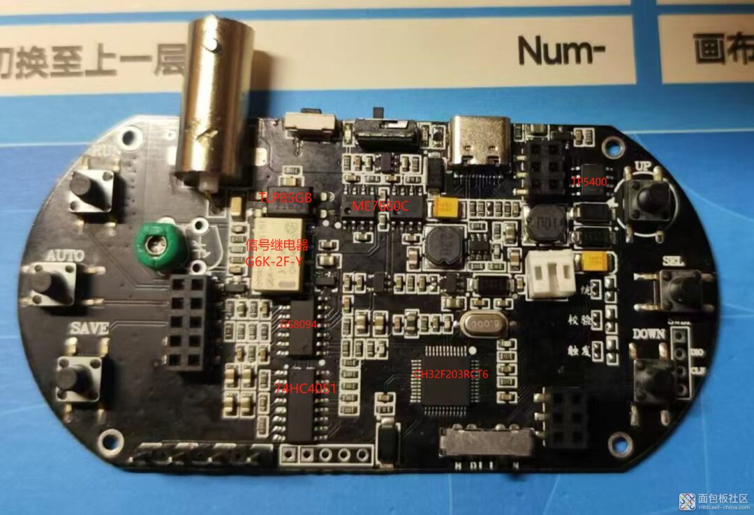
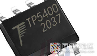
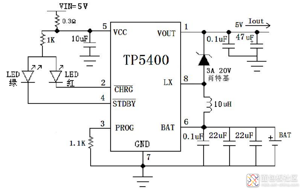
 Charging and Discharging Management Chip TP5400TP5400 is a single-cell lithium-ion battery charger and constant 5V boost controller dedicated to mobile power supplies, integrating high-precision voltage and charging current regulators, pre-charge, charging status indicators, and charging cutoff functions, capable of outputting a maximum charging current of 1A. The circuit design is also as simple as IP5306 and TP4054.
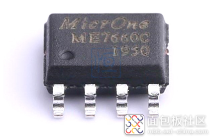
 Charge Pump Voltage Inverter ME7760CME7660 is a DC/DC charge pump voltage inverter integrated circuit, using mature AL gate CMOS technology and optimized design. The chip can convert an input voltage range of +1.5V to +10V into a corresponding -1.5V to -10V output, and only requires two low-loss capacitors without inductors. This reduces loss area and electromagnetic interference. The chip’s oscillator rated frequency is 10KHZ, and when applied in low input current situations, a capacitor can be connected between the oscillator and ground to operate normally at a frequency below 10KHZ.
 Features: 1. Convert logic power supply +5V to 5V dual-phase voltage 2. Wide input operating voltage range 1.5V to 10V 3. High voltage conversion accuracy 99.9% 4. High power conversion efficiency 98% 5. Low power consumption: static current is 90µA (when input is 5V) 6. Few external components, easy to use, only requires two external capacitors 7. 8-Pin DIP and 8-Pin SOIC small package 8. Complies with RS232 negative voltage standard 9. High electrostatic breakdown voltage of up to 3KV 10. No need for Dx diode when working at high voltage. Uses: I guess (1) When the voltage reverses, the oscilloscope can clearly display this reversal phenomenon, including the starting point of the reversal, duration, and voltage amplitude after the reversal, and other key parameters. (2) When the voltage signal reverses, the oscilloscope voltage inverter (or similar function) can capture and display this change.
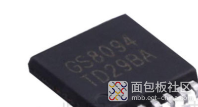
Operational Amplifier GS8094
Features: 1. Convert logic power supply +5V to 5V dual-phase voltage 2. Wide input operating voltage range 1.5V to 10V 3. High voltage conversion accuracy 99.9% 4. High power conversion efficiency 98% 5. Low power consumption: static current is 90µA (when input is 5V) 6. Few external components, easy to use, only requires two external capacitors 7. 8-Pin DIP and 8-Pin SOIC small package 8. Complies with RS232 negative voltage standard 9. High electrostatic breakdown voltage of up to 3KV 10. No need for Dx diode when working at high voltage. Uses: I guess (1) When the voltage reverses, the oscilloscope can clearly display this reversal phenomenon, including the starting point of the reversal, duration, and voltage amplitude after the reversal, and other key parameters. (2) When the voltage signal reverses, the oscilloscope voltage inverter (or similar function) can capture and display this change.
Operational Amplifier GS8094
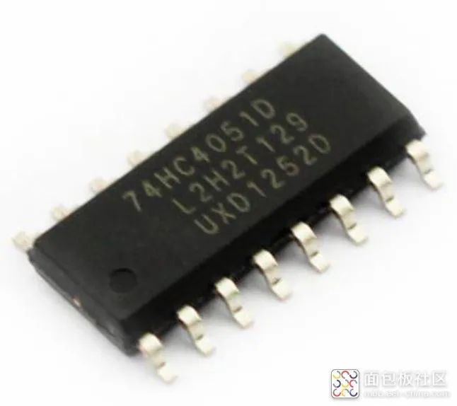
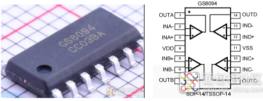 In my understanding (1) The operational amplifier can enhance weak signal amplitudes, making it easier to display and observe on the oscilloscope screen. (2) It performs preliminary amplification of input signals to ensure that the signal maintains sufficient amplitude and signal-to-noise ratio during subsequent processing. (3) High-quality operational amplifiers typically have extremely low noise levels, which helps reduce noise interference during measurements and improve measurement accuracy. Input offset voltage (Vos): 8mV Power Supply Rejection Ratio (PSRR): 80dB Storage Temperature: -55~+150℃ Package/Enclosure: SOP14_150MIL -3d Bandwidth: 350MHz Number of Channels: 4 Input Bias Current: 1pA Slew Rate: 232V/μs Gain Bandwidth Product (GBP): 195MHz Common Mode Rejection Ratio – CMRR: 80dB Output Type: Rail-to-Rail Operating Temperature: -40℃~+125℃ Dimensions: 8.63 x 3.90mm Height: 1.75mm Number of Pins: 14Pin Pin Pitch: 1.27mm8-Channel Analog Multiplexer 74HC4051D
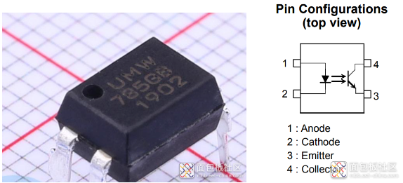
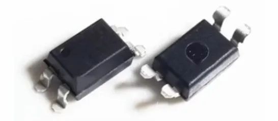
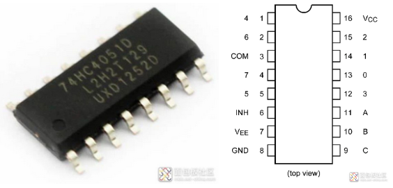 Wide operating temperature range: Topr =-40 to 125 ℃ Low power consumption: Icc = 4.0 µA (maximum) (Vcc = 6.0 V, VEe = GND, Ta = 25 ℃) Low on-resistance: RoN = 50 (typical value) at Vcc-VBg=9 V High linearity: THD = 0.02% (typical value) at Vcc -VBg=9 V. The multiplexer should summarize and process signals to improve accuracy.Isolation Voltage TLP785GBUsed to isolate high voltage components to prevent inputting 220V voltage from breaking down the main control chip.
Example Code: Due to the lack of code related to CH32 chips online, and since everyone is still mainly learning with STM32, I found an example program for STM32 to share with everyone to learn together.
Wide operating temperature range: Topr =-40 to 125 ℃ Low power consumption: Icc = 4.0 µA (maximum) (Vcc = 6.0 V, VEe = GND, Ta = 25 ℃) Low on-resistance: RoN = 50 (typical value) at Vcc-VBg=9 V High linearity: THD = 0.02% (typical value) at Vcc -VBg=9 V. The multiplexer should summarize and process signals to improve accuracy.Isolation Voltage TLP785GBUsed to isolate high voltage components to prevent inputting 220V voltage from breaking down the main control chip.
Example Code: Due to the lack of code related to CH32 chips online, and since everyone is still mainly learning with STM32, I found an example program for STM32 to share with everyone to learn together.
#define NPT 1024//Number of sampling points for a complete acquisition
/******************************************************************Function Name: GetPowerMag() Function Purpose: Calculate the amplitude parameters of each harmonic Note: First decompose lBufOutArray into real part (X) and imaginary part (Y), then calculate the amplitude (sqrt(X*X+Y*Y)*******************************************************************/void GetPowerMag(void){    float X,Y,Mag,magmax;//Real part, imaginary part, amplitude of each frequency, maximum amplitude    u16 i;    //Call self cr4_fft_1024_stm32  cr4_fft_1024_stm32(fftout, fftin, NPT);    //fftin is the Fourier input sequence array, fftout is the Fourier output sequence array      for(i=1; i<npt; 16)="" <<="" i++)="" x="(fftout" {="">> 16;    Y = (fftout >> 16);        Mag = sqrt(X * X + Y * Y);     FFT_Mag=Mag;//Store in cache for output verification    //Get the maximum frequency component and its amplitude    if(Mag > magmax)    {      magmax = Mag;      temp = i;    }    }  F=(u16)(temp*(fre*1.0/NPT));//There is an error in this formula in the source code, copy it here    LCD_ShowNum(280,180,F,5,16);}          </npt;>
u16 magout[NPT];/******************************************************************Function Name: InitBufInArray() Function Purpose: Initialize sine wave values, store the values of each point of the sine wave in magout[] array Parameter Description: Note:*******************************************************************/void InitBufInArray(void){ u16 i; float fx; for(i=0; i<npt; ******************************************************************function="" a="" dac_setchannel1data(dac_align_12b_r,magout);="" description:="" function="" i="0;" i++)="" i++;="" if(i="" in="" interrupt="" magout[i]="(u16)(2048+2048*fx);" name:="" note:="" of="" output="" parameter="" place="" purpose:="" simulate="" sine="" sinout()="" sinout(void){="" static="" the="" this="" timer="" to="" u16="" void="" wave="" wave*******************************************************************="" }="">=NPT) i=0;} </npt;>
Main Cost Analysis(1) Main control chip CH32F203CBT6. 8 yuan/piece
(2) LCD control chip CH32F203RCT6. 7 yuan/piece
(3) 2.4-inch LCD screen. 15 yuan
(4) TP5400. 0.5 yuan/piece
(5) ME7760C. 1 yuan/piece
(6) GS8094. 1.5 yuan/piece
(7) 74HC4051D. 0.5 yuan/piece
(8) TLP785GB. 0.5 yuan/piece
 Not including the shell, PCB board, etc. The prices of the more important chips add up to a pure cost of 34 yuan. What do you think about this cost? If we include other expenses, the cost of this product should be around 80-100 yuan. This can be considered a pretty good product.Conclusion(1) This mini oscilloscope, if your need is just to see a shape, to see what waveform it is, and it emphasizes portability, then this mini oscilloscope may help at critical moments. However, if you want to do projects and look at timing, then this mini oscilloscope is like a toy, and it is very troublesome to do projects and not very professional. (2) The overall workmanship of this mini oscilloscope is quite good, and it can be seen that a lot of effort was put into making this product. The LCD graphical interface is also very well done, and the two main chips used are both from Qingheng Microelectronics’ CH32 series. It can be considered a pretty good domestic product. (3) Suggestions for improvement include changing some buttons to wheels, as wheels would be much more convenient than buttons. Secondly, the shell could be made more aesthetically pleasing, perhaps using a silicone case to make it look more high-end. Finally, I hope a larger capacity battery can be fitted inside, as it emphasizes portability and the battery life must keep up.