System-on-Chip (SoC) is an integrated circuit that integrates a computing processor and other electronic systems into a single chip. SoCs can handle digital signals, analog signals, mixed signals, and even radio frequency signals, and are often used in embedded systems. Although microcontrollers (MCUs) typically have less than 100 kB of RAM, they are essentially a simplified, functionally limited SoC. The term “system-on-chip” is often used to refer to more powerful processor chips that can support running operating systems like Windows or Linux. High-performance SoCs integrate more and stronger functional modules, usually equipped with external memory, such as flash memory. Additionally, SoCs are often configured with many external interfaces to connect various external devices. To execute complex tasks more quickly, some SoCs also adopt multiple processor cores. The functionality, performance, and applications of SoCs are becoming increasingly complex, raising higher demands for chip design and wafer manufacturing.
Different types of SoCs have different application scenarios. SoCs built around microcontrollers (MCUs) are generally used in consumer electronics, home appliances, and IoT products that do not require high computing performance. SoCs based on microprocessors (MPUs) have relatively higher performance and functionality, such as the application processors (APs) in smartphones. There are also programmable SoCs (PSoCs), whose functions can be flexibly programmed, similar to FPGAs. Of course, SoCs that are custom-developed for specific application areas may be more complex, integrating functions such as ADC/DAC, display drivers, and wireless radio frequency modules.
Basic Components of SoC
A typical SoC structure includes the following components:
-
At least one microcontroller (MCU) or microprocessor (MPU) or digital signal processor (DSP), but there can also be multiple processor cores;
-
Memory can be one or more of RAM, ROM, EEPROM, and flash memory;
-
Oscillators and phase-locked loop circuits for providing timing pulse signals;
-
Peripherals composed of counters, timers, and power circuits;
-
Wiring interfaces of different standards, such as USB, FireWire, Ethernet, universal asynchronous receiver-transmitter, and serial peripheral interfaces;
-
ADC/DAC for converting between digital and analog signals;
-
Voltage conditioning circuits and regulators.
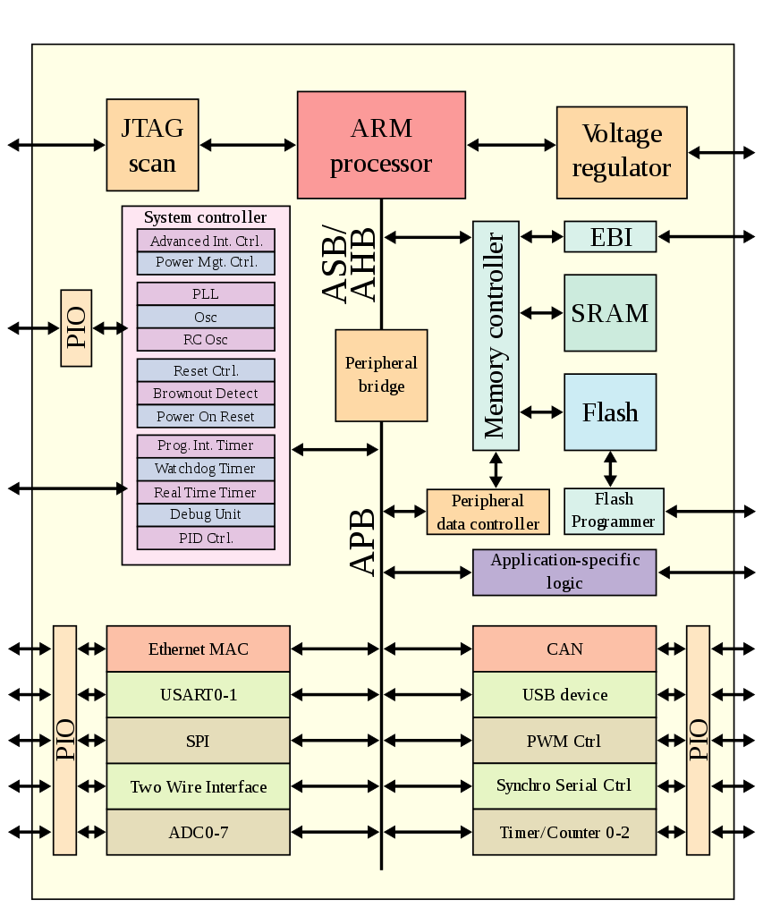
Figure 1: Schematic diagram of SoC structure based on microcontroller (MCU). (Source: Wikipedia)
Some SoCs also include wireless connectivity modules, such as Bluetooth, and the latest SoC designs even incorporate AI engines.
The flow of data mainly relies on the I/O bus in the system-on-chip, such as the AMBA standard provided by Arm. Using a DMA controller allows external data to be transferred directly to memory without going through the central processor, which can greatly improve data throughput efficiency. Over the past decade, a trend in SoC design has been to adopt network-based topologies to enhance on-chip communication efficiency. This routing-based packet interconnect network is called “Network-on-Chip” (NoC), which can overcome the bandwidth bottlenecks of traditional bus networks.
SoC Design Process
A complete system-on-chip consists of hardware and software components, where the software is used to control the hardware parts, including the microcontroller, microprocessor, or digital signal processor cores, as well as external devices and interfaces. The design process of SoCs mainly involves the co-design of hardware and software.
As the integration level of SoCs increases, design engineers must adopt reusable design ideas whenever possible. Most modern SoCs use predefined IP cores (including soft cores, hard cores, and firm cores) to complete rapid design in a reusable manner. In software development, the protocol stack is an important concept used to drive industry-standard interfaces like USB. In hardware design, designers typically use EDA tools to connect already designed (or purchased) IP cores together in an integrated development environment (IDE) to integrate various sub-functional modules.
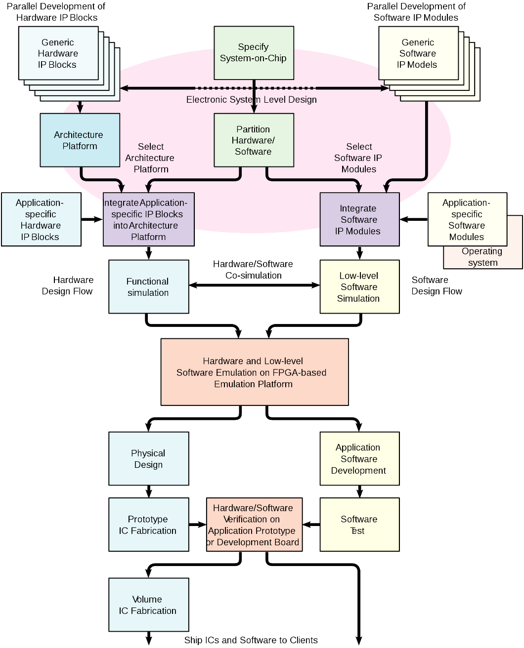
Figure 2: Schematic diagram of the SoC design process. (Source: Wikipedia)
Before the chip design is sent to the wafer factory for production, designers will adopt various methods to verify its logical functions. Simulation and verification are the most complex and time-consuming parts of the SoC design process, accounting for about 50% to 80% of the entire chip development cycle. Employing advanced design and simulation verification methods has become crucial for the success of SoC design.
Complex Design Choices for System-on-Chip (SoC)
The trend in SoC design is to base designs on SoC development platforms, which is a design approach that maximizes system reuse and is integration-oriented, allowing for the sharing of IP core development and system integration results, continuously reshaping the value chain. While focusing on area, delay, and power consumption, the emphasis shifts towards yield, reliability, EMI noise, cost, and ease of use, rapidly enhancing system-level integration capabilities.
SoC design engineers face many choices, including processor cores, various IP modules, EDA tools and development environments, as well as RF modules, Network-on-Chip (NoC), and FPGAs. Making the best choices that align with their application and design needs has become a significant challenge. To address this, “Electronic Engineering Magazine” interviewed technical and design experts from processor core, EDA and IP, NoC vendors, as well as FPGA and SoC chip design companies, who provided in-depth and unique insights from their perspectives.

EDA and IP
Vice President of Synopsys China, Xie Zhonghui
What functional modules or IP are generally included in mainstream SoCs? What new technology trends are worth paying attention to?
In high-performance computing, consumer electronics, communications, and automotive applications, SoC is a major chip product form. The biggest difference between SoC and ASIC is that it forms a complete system on a chip, which includes computing, storage, peripherals, and hierarchical bus subsystems, thus achieving a complete computer system architecture on a single chip.
These key subsystems of SoCs will adopt different types of IP based on different system specifications and application scenarios. The computing subsystem typically includes CPU, GPU, and AI processors as homogeneous or heterogeneous computing units. The storage subsystem usually adopts large-capacity external dynamic random-access memory standards such as DDR/LPDDR/HBM/GDDR, as well as SRAM-based static high-speed on-chip memory. The types of external device interface IP are even more diverse, and various buses we encounter in our daily lives are likely to appear in system chips. Among these, PCI Express (CXL/CCIX), HBI, and other interface standards are responsible for high-performance system expansion functions, enabling high-speed peripherals, Die-to-Die, or multi-chip interconnections. Currently, PCI Express is evolving to the latest 6.0 version, while CXL has evolved to version 1.2. Additionally, there are specialized interface buses tailored to specific application needs, including USB, SATA, MIPI, DisplayPort, HDMI, UFS, and Ethernet, among many other technical standards. The new generation USB4 has entered the public eye with Apple’s adoption of its self-developed M1 chip in the MacBook, offering a maximum transmission rate of 40Gbps. DisplayPort is also developing towards the 2.0 standard, ultimately supporting multiple ultra-high-definition display outputs with a bandwidth of 80Gbps. The MIPI bus is also responding to the higher demands posed by mobile communications, multimedia, and automotive applications, gradually moving towards diversification.
The on-chip bus subsystem is like the central nervous system of the SoC, responsible for achieving high-speed interconnection and collaborative work between various subsystem modules. The on-chip bus is categorized into star, ring, and mesh connections based on different topologies. The specific bus structure to be adopted requires complex simulation analysis based on design goals. Currently, with the rapid development of artificial intelligence technology, hybrid bus systems based on various bus topologies are also gradually developing.
What role can AI play in complex high-performance SoC design? What are the future design trends?
The complex high-performance SoC design process has infinite design parameters to explore, such as module layout, design size and shape, and countless EDA automation tool processes and variables to try. The design exploration phase can significantly impact the final result, so design teams often invest substantial human and machine resources during this phase, spending most of the overall design time. Advances in AI and ML technology can significantly accelerate the speed of design exploration, such as Synopsys’ DSO.ai and ML technologies built into design implementation tools, which not only achieve design goals faster but also reduce the human and machine resources needed during the exploration process.

FPGA
General Manager of Lattice Semiconductor China, Guo Jing
What major factors need to be considered when planning SoC design?
I believe it is essential to start from market demand and the related timing window, then consider one’s own human and technical resources, combined with the costs of development, time, and maintenance, to choose the processes and IP. For example, if one is still using 40nm process technology to design SoCs, it will be challenging to meet the market’s general demand for low power consumption. However, if using advanced process SoCs, the selection of IP under the new process is relatively low, costs are high, and reliability and compatibility are also uncertain. It is evident that whether an SoC can succeed at once involves numerous interrelated risks, posing significant challenges to controlling the overall input-output ratio. Therefore, this gives rise to the very important factor of reducing risks and accelerating time-to-market.
By utilizing existing relatively low-performance but low-power processors, implementing already validated high-performance IP modules (or even multiple soft-core processors) using low-power, small-area FPGAs, and then integrating them through advanced packaging technology, a programmable SoC can be created that can be updated at any time. For example, Lattice’s “iCE” platform is an excellent solution that can reduce risks and speed up time-to-market.
How do RISC-V and FPGA organically combine to assist SoC design?
RISC-V has a rich ecosystem, and its soft-core form relies on FPGA, enabling FPGA to immediately possess these rich ecosystem resources. Optimized RISC-V not only reduces resource consumption on FPGAs but also, through the diversity of peripherals, grants FPGAs quicker scheduling and configuration capabilities for each functional module in parallel algorithm applications. FPGAs excel in high-performance parallel applications, and adding RISC-V allows for multi-image loading, network protocol stitching, and even applications integrating multiple independent RISC-V.
Current soft-core RISC-V has excellent portability across platforms. Many embedded applications, such as those based on ARM Cortex M4, still face certain challenges when integrated into low-cost FPGAs. The good news is that Lattice’s second-generation Titanium series FPGA with 16nm process technology can easily achieve 450MHz, allowing the soft-core RISC-V processor to compete with the hard-core Cortex M4 processor. Moreover, under equivalent performance, all RISC-V buses are embedded in FPGA in AXI form, bringing additional value such as high flexibility, quick time-to-market, and extremely low IP integration risks.

RISC-V Processor Core
Senior Director of Sifive Technology Co., Ltd., Wu Jun
What standards are mainstream SoCs based on when selecting processor core IP? How to achieve differentiated design?
There are many standards for this, but we believe that two standards need to be emphasized. The primary standard is whether the processor core IP fully supports Linux, as general embedded, industrial, IoT, high-performance real-time embedded, and automotive fields all require running on Linux systems. For example, Sifive’s U5, U7, and U8 series processor core IP are all based on RISC-V architecture and support the Linux operating system, configured with cache hierarchy structures to balance area performance, achieving high performance and high energy efficiency requirements.
The second standard is to select pipeline stages, issue counts, etc., based on performance indicators, and choose the instruction set required by application needs, such as whether floating-point computation is needed, and whether it supports double-precision floating-point computation. These standards will all impact the selection of processor core IP.
For Sifive Technology, differentiated design of SoCs mainly reflects in two aspects. First, the selection of IP based on application scenarios and self-developed IP to achieve the best performance-to-power ratio. Different application scenarios require chips with various functions, so the demand for chips is more diversified. We will choose corresponding IP based on application scenarios, while also combining self-developed IP to achieve the best balance, thus realizing differentiated design of SoCs.
The second aspect is providing customers with a software development platform that enables rapid deployment at the software level. For vertical domain chips, Sifive Technology currently has three mature innovative custom platforms: an intelligent voice processor platform, an intelligent vision processor platform, and a low-power BLE processor platform. Recently, Sifive Technology released the world’s first RISC-V-based AI vision processor platform “Jinghong 7100,” which has generated a huge response. Customers can quickly customize chip products for target application scenarios based on the specifications of this platform, and the platform also supports continuous optimization, updates, and iteration of chips, thereby significantly shortening the chip development cycle and quickly realizing the application of customers’ innovative technologies.
What new technologies and application trends in SoC design are worth paying attention to?
First, heterogeneous multi-core computing technology. With the maturity of AI applications and technologies, the demand for efficient, reliable, and stable operation and computation for AI terminals is increasing day by day. Different application scenarios have varying demands for chip PPA, and a single core can no longer meet the multi-path multi-computation flow required for AI applications while considering power consumption and computational resources.Therefore, heterogeneous multi-core computing technology has become the best solution to address these applications.
Second, chiplet packaging technology. With the rapid development of integrated circuit manufacturing technology, integrating a complete electronic system into a single chip, known as system-on-chip (SoC), can significantly improve system reliability, reduce system area and power consumption, and lower system costs. However, with the development of AI and 5G, traditional design methods can no longer meet the functional requirements of these chips. Cutting a SoC design into smaller chips (Chiplets) suitable for different process nodes and then packaging multiple Chiplets in the same package using advanced packaging technology will be the future trend.
Finally, it is important to mention NoC bus interconnect technology. As mentioned earlier, emerging applications such as AI and 5G impose higher requirements on chip design. SoC design methods can no longer meet the design requirements of these chips. With the development of integrated circuits, Network-on-Chip (NoC) as a new design methodology effectively addresses the communication bottlenecks of single bus SoCs. However, it also has many issues that need to be resolved, such as complex internal interconnections and significant crosstalk phenomena. Therefore, this is also an area that needs research and attention in the future.
What challenges does current SoC design face in terms of performance, power consumption, and size? What are the solutions?
First, there are physical implementation challenges under advanced processes, such as complex back-end implementation processes below 16nm. Second, complex SoCs require the integration of a large number of physical IPs, which makes verification more difficult. Finally, there is uncertainty in computational density for complex systems, mainly reflected in AI computing.
Solutions to the first two challenges lean towards using chiplet integration to design SoCs, thereby reducing complete dependence on process nodes and addressing the verification difficulties associated with integrating large amounts of physical IP.
For the last challenge, advanced design methodologies need to be employed to design IP. Sifive Technology’s solution is to use an agile design methodology called Chisel, a hardware construction language based on Scala, which has been widely accepted in academia and industry for generating RTL for digital IC design. Its high-density code, better support for objects and high-level languages, rapid development speed, short cycle, and high reusability can achieve determinacy in computational density for complex systems.

Network-on-Chip (NoC)
CTO of Arteris IP, Benoit de Lescure
What is Network-on-Chip (NoC)? Why do SoC designs need NoC?
Before introducing the history of NoC, I would like to make a point: NoC is a SoC architecture. Literally, NoC is the logical and physical instance connecting IP modules drawn by SoC architects in their block diagrams and floor plans. So many SoC design teams obtain IP module licensing from companies like Arm, Synopsys, and Cadence, leading to homogenization in SoC designs. The key to achieving differentiated SoC design lies in how architects select and connect these IP modules to meet their system-level requirements.
What are the advantages and disadvantages of Network-on-Chip (NoC) compared to traditional bus interface communication?
The number of IP modules contained in SoCs is constantly increasing, while the complexity of on-chip quality of service (QoS), arbitration, and data flow optimization is also rising. NoC is gradually replacing buses and crossbars, becoming the industry standard for on-chip interconnect. Buses are shared communication resources, and except for the simplest systems, buses cannot provide the bandwidth required by the system. Crossbars can provide sufficient bandwidth, but their size grows exponentially with the number of connected IP modules, and large crossbars are impossible to construct. They also do not make good use of wiring, which is the most expensive aspect of today’s chip technology. NoC can significantly reduce die area (especially with less wiring), lower power consumption, and fine-tune and optimize on-chip data flow and quality of service, even providing data protection functions to enhance the overall system’s functional safety.
Buses were the standard adopted in the early stages of SoC development when the number of connected IP modules (CPUs, memory, and peripheral controllers, etc.) was no more than 20. However, as more IP modules connected to the bus, they began competing for priority and available bandwidth. Buses require centralized arbitration and address decoding logic, and as the number of hosts and slaves increases, they all compete for the same bus resources, which has become a bottleneck for SoC performance.
What challenges do high-performance SoC designs face in terms of performance, power consumption, and size?
Currently, most high-performance SoC designs use advanced process nodes below 10nm, where the size of transistors can be reduced to incredible levels. This allows for the integration of billions of transistors onto a single die, whereas a few years ago, the same-sized die could only accommodate hundreds of millions of transistors. However, the width of metal lines has not shrunk to the size of transistors, and as more IP modules are added to the system, the number of metal lines required to connect them increases, as does the distance data must travel on the chip. For SoC designs from five years ago, NoC might have accounted for 10% of the die area, but in today’s advanced high-performance SoCs, this area ratio is increasing. However, we are also continuously improving NoC technology to enable it to operate at high clock frequencies and high voltages for high-performance applications. When NoC does not require high bandwidth, we can quickly and transparently “throttle” it down to energy-saving mode. NoC technology provides many “levers” that SoC architects can use to optimize for specific performance, power consumption, and area requirements.

RISC-V and SoC Design Platforms
CEO of Xilinx Technology, Peng Jianying
What major factors need to be considered when planning SoC design?
As a CPU IP supplier, we have observed from various customers that the major factors they consider when planning SoC design include:
a) Product definition and key technical indicators: Generally, customers have targeted markets and application scenarios, so early product definitions are relatively clear, such as specific performance requirements (frequency, DMIPS/CoreMark scores) for the CPU, as well as a list of required peripheral IPs and overall chip frequency, area, and power consumption.
b) Hardware characteristics and overall architecture: Once the product definition is determined, the next step is to define software and hardware functions, determine hardware module characteristics, and the overall SoC architecture (main bus structure). This involves assessing the entire SoC architecture through specific applications and algorithms, including bus structure, the number of masters/slaves and their connections, storage structure, and specific characteristics of key IP modules. For the CPU, it needs to be determined whether DSP, FPU, etc., processing units are required; the storage structure (ICache/DCache, on-chip instruction tightly coupled SRAM, on-chip data tightly coupled SRAM) and size, as well as the required system bus structure.
c) Software ecosystem and user habits: The software ecosystem and user habits are intangible yet crucial for SoC design. The software development environment (IDE, SDK, etc.), basic toolchain (compiler, debugger, etc.), and operating system support levels all relate to the efficiency and habits of software development for chip end customers.
d) Cost-effectiveness of time, human resources, and funding: High cost-effectiveness is a necessary condition for commercial customer success. Everyone hopes to complete SoC software and hardware design and verification in the shortest time and with the least human resources, while also hoping that IP costs, subsequent wafer production, packaging, and testing costs are all at reasonable prices.
Of course, each customer may prioritize or weigh these factors differently. Since its establishment two years ago, Xilinx Technology has witnessed the blossoming of RISC-V in China. Initially, most SoC design companies were cautious about RISC-V due to software ecosystem and user habits. With the vigorous development of the RISC-V ecosystem, we now see more and more customers choosing RISC-V for its cost-effectiveness, differentiated product definitions, and flexible scalability.
What standards do mainstream SoCs base their selection of processor core IP on? How to achieve differentiated design?
When designing SoCs, there are indeed certain unified standards for selecting processor IP, such as hardware indicators, software indicators, stability, and price.
Hardware indicators mainly include:
-
Frequency, area, and power consumption requirements under specific processes, as well as typical CPU benchmark scores (DMIPS, CoreMark, etc.);
-
Different instruction set combinations, such as RISC-V 32-bit or 64-bit instruction sets, DSP, single and double precision FPU, etc.;
-
Storage unit structure and size;
-
Number of interrupts and priorities, response speed, etc.;
-
Supported bus interface types and clock frequency ratios.
Software indicators mainly include:
-
A complete software development environment and development platform (IDE, SDK, etc.);
-
A mature and stable toolchain (compiler, simulator, debugger, etc.);
-
Standard software interfaces and a rich algorithm software library;
-
Friendly third-party software support (Segger, IAR, Lauterbach, etc.);
-
Support for mainstream operating systems (RTOS, Linux, etc.).
Stability mainly refers to the need for CPU IP to be sufficiently validated across different processes and testing platforms to ensure robustness. Price mainly includes licensing fees and subsequent support and maintenance costs.
How to provide customers with competitively differentiated designs? This has always been a direction of exploration and effort for Xilinx Technology. Currently, we mainly consider the following aspects:
1) Highly configurable processor IP
All RISC-V CPU IPs from Xilinx include rich configurable options, allowing customers to configure the parameters they need through a graphical interface to meet performance requirements without wasting additional resources, such as the number and priority of interrupts, ICache/DCache size, whether on-chip instruction and data SRAM are needed, multiplication cycle counts, etc. The required code is then generated.
2) Scalability of the RISC-V instruction set (user-defined instructions)
The RISC-V instruction set definition has reserved some encoding space for user-defined instructions. Xilinx provides the NICE (Nuclei Instruction Co-Unit Extension) extension solution. Customers can analyze the algorithms that need hardware acceleration based on specific application fields and define corresponding instructions, using the NICE interface reserved in the Xilinx RISC-V processor microkernel to realize acceleration units for specific fields. These acceleration units can share resources such as storage with the processor microkernel, significantly improving energy efficiency and helping customers quickly develop differentiated products for specific field architectures.
3) Hardware acceleration modules for specific fields
For certain niche SoC designs, Xilinx Technology also provides various flexible hardware acceleration solutions, such as processor physical security enhancement modules, dual-core lockstep, vector modules, and NPU modules.
What new technologies and application trends in SoC design are worth paying attention to?
With the arrival of the 5G and AIoT era, more and more intelligent application scenarios are emerging, leading to the trend of “application and software-defined chip SoC design,” which poses new requirements for rapid product iteration. This means that SoC design needs to:
-
More effectively solve practical problems in specific scenarios
-
Faster market response speed
-
Possess differentiated characteristics and cost advantages
I believe that current SoC design mainly has the following key trends:
1) DSA (Domain Specific Architecture or Domain Specific Accelerator), co-processor accelerators for specific application fields
The goal of DSA is to enhance the energy efficiency ratio of computing, thus better meeting the differentiation, security, and timeliness requirements of SoC design. How to achieve this goal? One core concept is “specialization in the field,” which means using specialized hardware to meet specific field needs. However, this differs from general ASIC hardwareization, as DSA aims to meet the needs of a field and solve a class of problems rather than a single problem, thus achieving a balance between flexibility and specialization. In the processor field, DSA can be interpreted as Domain Specific Accelerator, which expands certain accelerators for specific fields based on general processing to enhance efficiency in solving problems in that field.
2) Full-stack SoC design platformization
Full-stack SoC design platformization can significantly reduce the traditional SoC design cycle and cost. A one-stop SoC platform can provide overall solutions for SoC software and hardware design, generally including basic common IP required for SoC design, SoC architecture, test cases, operating systems, software drivers, algorithm libraries, and development tools. Currently, Xilinx Technology has launched a full-stack IP overall solution based on Xilinx RISC-V processors for applications in MCU, AIoT, etc., including pre-integrated overall SoC templates (containing Xilinx’s basic IP library, unified IP interfaces, and bus structures, etc.), software and hardware drivers, NMSIS algorithm libraries, complete ported operating system examples, and Xilinx’s own IDE/SDK, etc. This ensures that customers can customize SoC designs as needed without wasting resources, helping them reduce R&D investment and improve R&D efficiency and quality. The Xilinx full-stack IP platform can undertake 80% of the general SoC design verification work, allowing customers to focus more on the 20% of specialized SoC design.
3) The new IP reuse model of chiplet
In the post-Moore’s Law era, chip integration is becoming increasingly high, and SoC design is becoming more complex. To reduce the overall design cycle and total development cost of the chip SoC, the chiplet model has become a popular trend. A chiplet is essentially a die with specific functionality. Based on the chiplet model, the complex functions to be realized are first decomposed, then different dies with different process nodes, materials, and functions are developed or reused, and finally, a complete chip is formed through SiP (System in Package) packaging technology. Therefore, chiplet represents a new IP reuse model—providing it in the form of die.
Chiplet can not only solve the misalignment of digital circuits and analog or interface circuits in process nodes but also provide greater flexibility for SoC design. For example, some SoC designs have varying requirements for the number of interfaces or analog channels in different scenarios. Integrating everything onto one die lacks flexibility, making it difficult to optimize performance, functionality, and area (PPA). Chiplet better addresses the flexibility issues of digital and analog circuits in various scenarios. However, chiplet also faces many challenges, such as interface standardization and the high power consumption caused by the large data volume between dies.
What are the differences in SoC design requirements between IoT and edge computing compared to mobile computing/personal computers? How to choose the appropriate processor core?
From personal computers to mobile computing (smartphones), chip SoC design (including processor development) has primarily been driven by single applications and key products. However, with the emergence of various application scenarios like 5G, AIoT, and edge computing, and the lack of clear industry standards and specifications, application scenarios are becoming more diverse, demands more fragmented, single product demand moderate, and innovation iterations faster, requiring quicker market response speeds. Therefore, customized SoC design has become a trend. As the brain of the entire SoC, the processor’s selection goes beyond traditional PPA hardware indicators, complete basic software toolchains, and ecosystems, placing greater emphasis on the flexibility and scalability of the processor to meet differentiated and diverse designs, as well as establishing technological barriers.
ARM does not have absolute ecological advantages in these emerging fields; thus, RISC-V, which is open and has advantages in terms of simplicity, low power consumption, modularity, and scalability, will have significant opportunities in AIoT, edge computing, and other areas requiring customization.
In addition to technical flexibility, RISC-V can also provide significant cost advantages for AIoT, edge computing, and other fields. According to the market analysis report by international market research firm Semico Research titled “RISC-V Market Analysis: Emerging Markets,” it is expected that by 2025, the market will consume a total of 62.4 billion RISC-V CPU cores, with China having the world’s largest market space.
Xilinx Technology has released ultra-low-power N100, N200, N300 series, as well as high-performance 600 and 900 series (including 32-bit and 64-bit architectures) RISC-V processor IP products. These not only have rich configurable options that allow customers to choose flexibly but also provide specific selectable features for certain vertical niche areas. We hope to lead the RISC-V open ecosystem and empower AIoT innovation transformation together with domestic customers.
↓↓ Scan the code to participate in the High-Performance Passive Component Development Forum ↓↓